DESCRIPTION
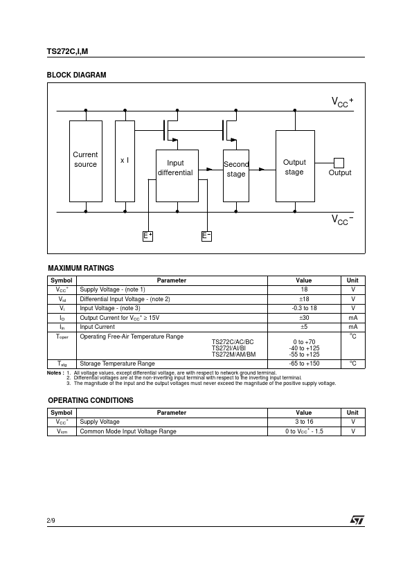
Three power consumptions are available allowing to have always the best consumption-speed ratio : q ICC= 10µA/amp. : TS27L2 (very low power) q ICC= 150µA/amp. : TS27M2 (low power) q ICC= 1mA/amp. : TS272 (high speed) These CMOS amplifiers offer very high input impedance and extremely low input currents. The major advantage versus JFET devices is the very low input currents drift with temperature (see figure 2). August 1998 PIN CONNECTIONS (top view) 1 2 3 4 + + 8 7 6 5 1 - Output 1 2 - Inverting Input 1 3 - Non-inverting Input 1 4-V CC 5 - Non-inverting Input 2 6 - Inverting Input 2 7 - Output 2 8 - V CC + 1/9 TS272C,I,M BLOCK DIAGRAM VCC Current source xI Input differential Second stage Output stage Output VCC E E MAXIMUM RATINGS
Symbol VCC+ Vid Vi IO Iin Toper Supply Voltage - (note 1) Differential Input Voltage - (note 2) Input Voltage - (note 3) Output Current for VCC+ ≥ 15V Input Current Operating Free-Air Temperature Range TS272C/AC/BC TS272I/AI/BI TS272M/AM/BM Tstg Storage Temperature Range 0 to +70 -40 to +125 -55 to +125 -65 to +150 o Parameter Value 18 ±18 -0.3 to 18 ±30 ±5 Unit V V V mA mA o C C Notes : 1. STMicroelectronics