TS274BI
TS274BI is HIGH SPEED CMOS QUAD OPERATIONAL AMPLIFIERS manufactured by STMicroelectronics.
DESCRIPTION
The TS274 series are low cost, low power quad operational amplifiers designed to operate with single or dual supplies. These operational amplifiers use the SGS-THOMSON silicon gate CMOS process allowing an excellent consumption-speed ratio. These series are ideally suited for low consumption applications. Three power consumptions are available allowing to have always the best consumption-speed ratio : q ICC= 10µA/amp. : TS27L4 (very low power) q ICC= 150µA/amp. : TS27M4 (low power) q ICC= 1m A/amp. : TS274 (high speed) These CMOS amplifiers offer very high input impedance and extremely low input currents. The major advantage versus JFET devices is the very low input currents drift with temperature (see figure 2).
October 1997
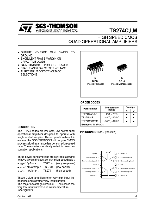
PIN CONNECTIONS (top view)
Output 1 1 Inverting Input 1 2 Non-inverting Input 1 3 VCC + 4 Non-inverting Input 2 5 Inverting Input 2 6 Output 2 7 + + + +
14 Output 4 13 Inverting Input 4 12 Non-inverting Input 4 11 VCC 10 Non-inverting Input 3 9 8 Inverting Input 3 Output 3
1/8
TS274C,I,M
BLOCK DIAGRAM
Current source x I
Input differential
Second stage
Output stage
Output
MAXIMUM RATINGS
Symbol VCC+ Vid Vi IO Iin Toper Supply Voltage
- (note 1) Differential Input Voltage
- (note 2) Input Voltage
- (note 3) Output Current for VCC+ ≥ 15V Input Current Operating Free-Air Temperature Range TS274C/AC/BC TS274I/AI/BI TS274M/AM/BM Tstg Storage Temperature Range 0 to +70 -40 to +125 -55 to +125 -65 to +150 o
Parameter
Value 18 ±18 -0.3 to 18 ±30 ±5
Unit V V V m A m A o
Notes : 1. All voltage values, except differential voltage, are with respect to network ground terminal. 2. Differential voltages are at the non-inverting input terminal with respect to the inverting input terminal. 3. The magnitude of the input and the output voltages must never exceed the magnitude of the positive supply voltage.
OPERATING CONDITIONS
Symbol VCC
+
Parameter Supply Voltage mon Mode Input Voltage Range
Value 3 to 16 0 to VCC...