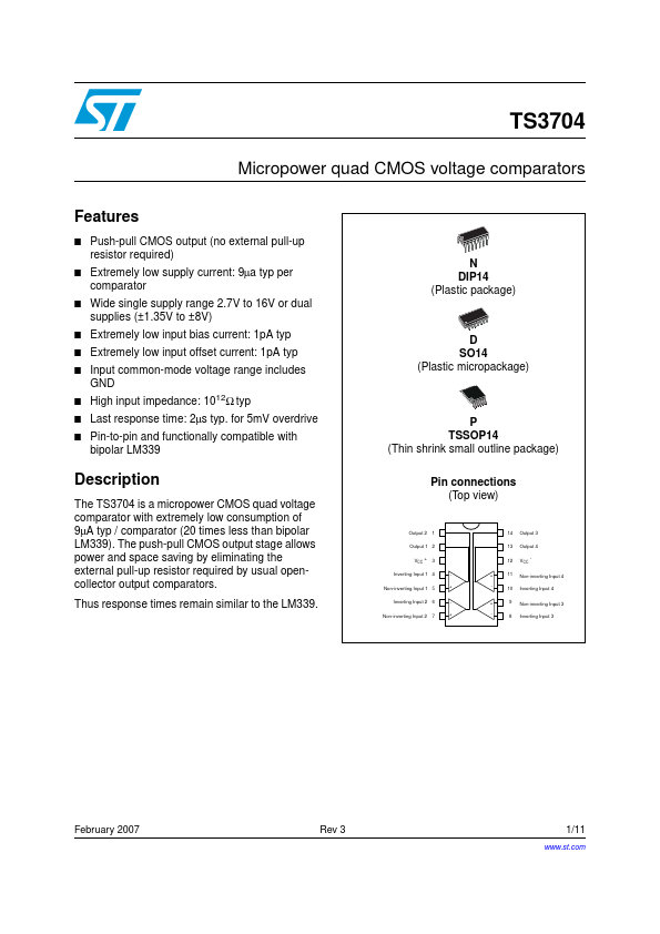
DESCRIPTION
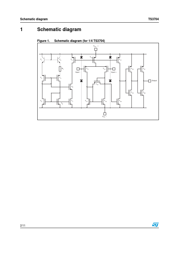
Thus response times remain similar to the LM339. January 1999 Inverting Input 1 4 Non-inverting Input 1 5 Inverting Input 2 6 Non-inverting Input 2 7 1/6 TS3704C,I,M SCHEMATIC DIAGRAM (for 1/4 TS3704) VCC + T 10 T1 T2 T9 T 17 R1 Input T3 T4 T 11 T 12 Input + T 18 T 21 Output T 13 T8 T 19 T 20 T5 T6 T7 T14 T15 T 16 VCC - MAXIMUM RATINGS
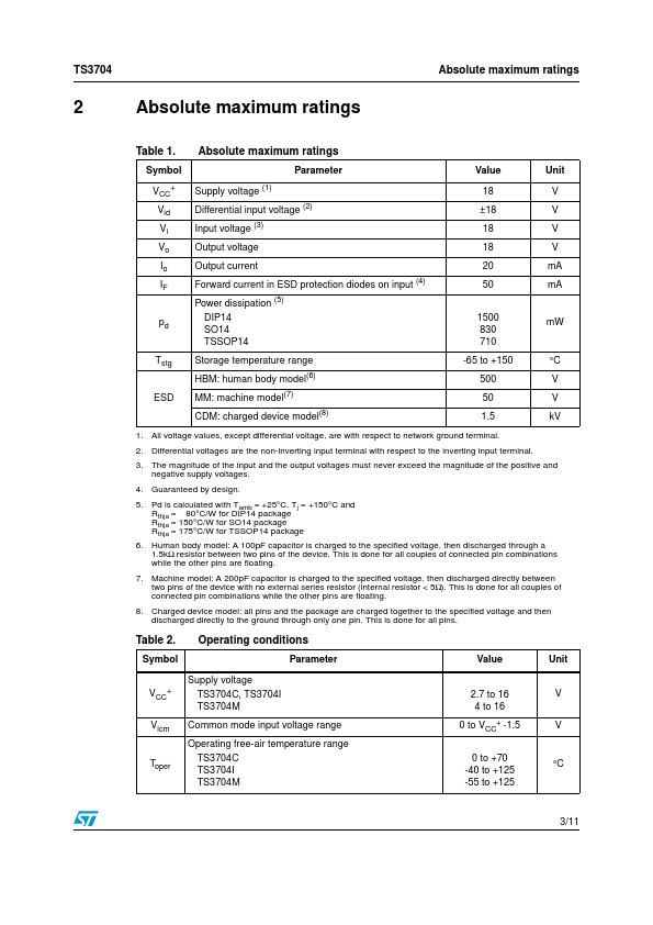
Symbol VCC+ Vid Vi VO IO Toper Supply Voltage - (note 1) Differential Input Voltage - (note 2) Input Voltage - (note 3) Output Voltage Output Current Operating Free-Air Temperature Range TS3704C TS3704I TS3704M Tstg Notes : 1. 2. 3. 4. Parameter Value 18 ± 18 18 18 20 0 to +70 -40 to +125 -55 to +125 -65 to +150 Unit V V V V mA o C Storage Temperature Range o C All voltage values, except differential voltage, are with respect to network ground terminal. Differential voltages are the non-inverting input terminal with respect to the inverting input terminal. The magnitude of the input and the output voltages must never exceed the magnitude of the positive supply voltage. STMicroelectronics