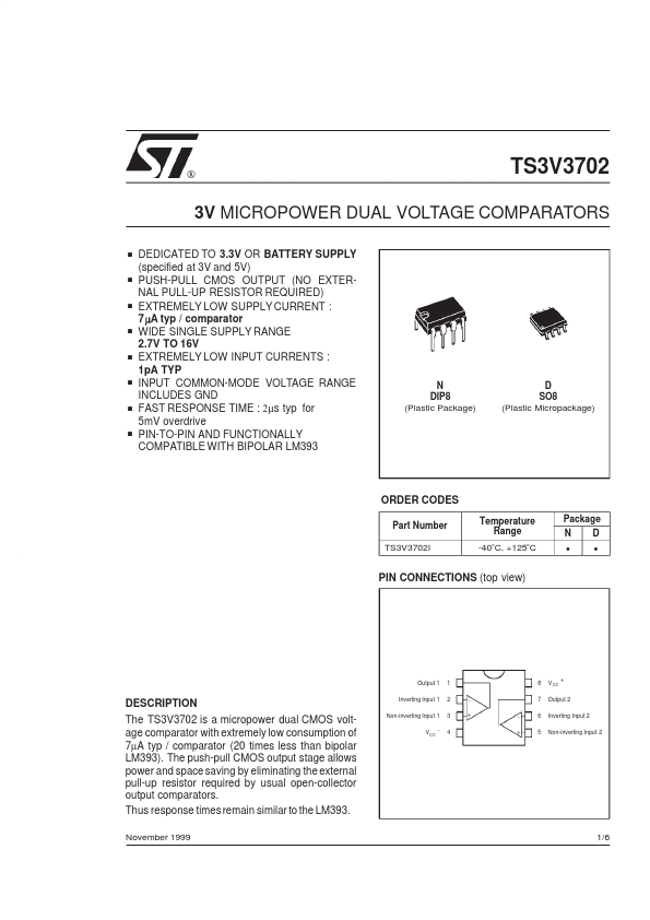
DESCRIPTION
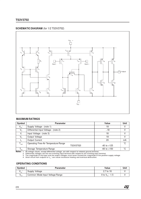
Thus response times remain similar to the LM393. November 1999 Inverting Input 1 Non-inverting Input 1 VCC - 1/6 TS3V3702 SCHEMATIC DIAGRAM (for 1/2 TS3V3702) VCC + T10 T1 T2 T9 T17 R1 Input T3 T4 T11 T12 Input + T18 T21 Output T 13 T8 T19 T20 T5 T6 T7 T14 T15 T16 VCC - MAXIMUM RATINGS
Symbol VCC Vid Vi VO IO Toper Tstg Notes : 1. 2. 3. 4. + Parameter Supply Voltage - (note 1) Differential Input Voltage - (note 2) Input Voltage - (note 3) Output Voltage Output Current Operating Free-Air Temperature Range TS3V3702I Storage Temperature Range Value 18 – 18 Unit V V V V mA o 18 18 20 -40 to +125 -65 to +150 C C o All voltage values, except differential voltage, are with respect to network ground terminal. Differential voltages are the non-inverting input terminal with respect to the inverting input terminal. The magnitude of the input and the output voltages must never exceed the magnitude of the positive supply voltage. Short circuit from outputs to VCC+ can cause excessive heating and eventual destruction. STMicroelectronics