DESCRIPTION
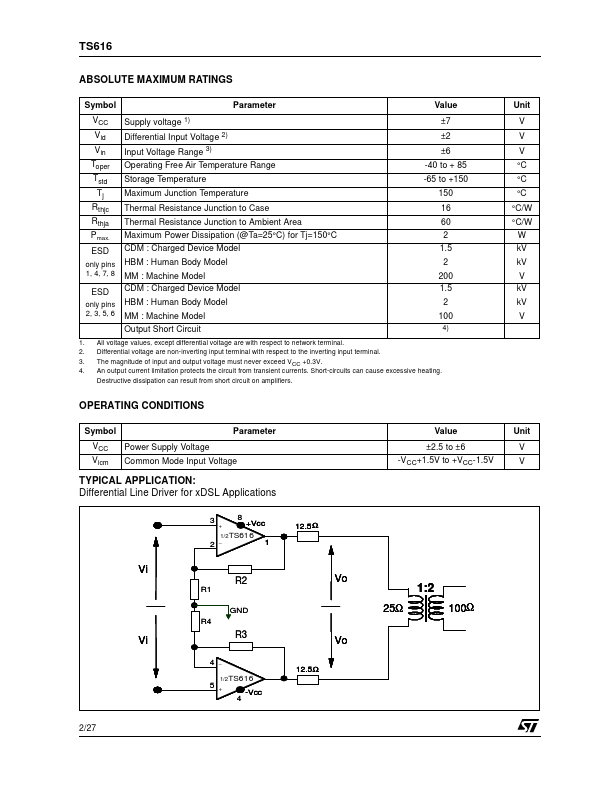
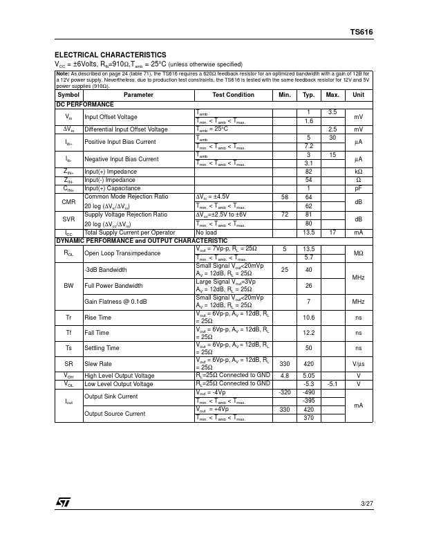
This circuit is capable of driving a 10 Ω or 25 Ω load at ±2.5V, 5V, ±6V or +12V power supply. The TS616 is able to reach a -3dB bandwidth of 40MHz on 25Ω load with a 12dB gain. This device is designed for high slew rates supporting low harmonic distortion and intermodulation. ORDER CODE Part Number TS616IDW TS616IDWT Temperature Range -40, +85°C -40, +85°C Package DW DW DW = Small Outline Package with Exposed-Pad, T = Tape & Real PIN CONNECTIONS (top view) Output1 1 Inverting Input1 2 Non Inverting Input1 3 VCC - 4 8 VCC + + 7 Output2 + 6 Inverting Input2 5 Non Inverting Input2 APPLICATION Cross Section View Showing Exposed-Pad This pad can be connected to a (-Vcc) copper area on the PCB s Line driver for xDSL s Multiple Video Line Driver December 2002 1/27 TS616 ABSOLUTE MAXIMUM RATINGS
Symbol VCC Vid Vin Toper Tstd Tj Rthjc Rthja Pmax. ESD only pins 1, 4, 7, 8 Parameter Supply voltage 1) 2) Value ±7 ±2 ±6 -40 to + 85 -65 to +150 150 16 60 2 1.5 2 200 1.5 2 100 4) Unit V... STMicroelectronics