DESCRIPTION
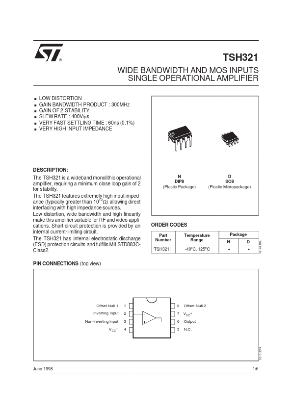
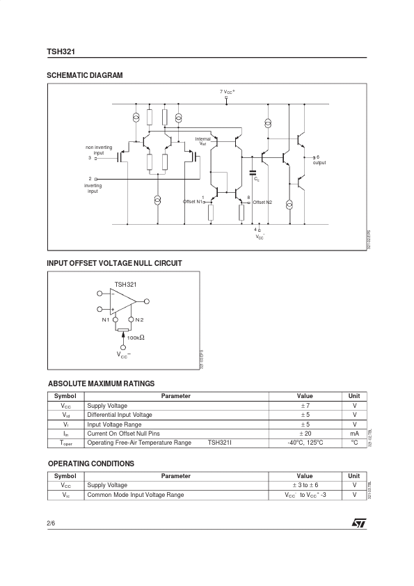
: Low distortion, wide bandwidth and high linearity make this amplifier suitable for RF and video applications. Short circuit protection is provided by an internal current-limiting circuit. N DIP8 (Plastic Package) D SO8 (Plastic Micropackage) ORDER CODES Part Number Temperature Range Package N D TSH321 SCHEMATIC DIAGRAM 7 V CC + non inverting input 3 Internal Vref 6 output Cc 2 inverting input 1 Offset N1 8 Offset N2 INPUT OFFSET VOLTAGE NULL CIRCUIT TSH321 N1 N2 100kΩ V CC ABSOLUTE MAXIMUM RATINGS
Symbol VCC Vid Vi Iin Toper Supply Voltage Differential Input Voltage Input Voltage Range Current On Offset Null Pins Operating Free-Air Temperature Range TSH321I Parameter Value ±7 ±5 ±5 ± 20 -40oC, 125oC Unit V V V mA o 321-02.TBL 321-03.TBL 321-03.EPS C OPERATING CONDITIONS Symbol VCC Vic Supply Voltage Common Mode Input Voltage Range Parameter Value ± 3 to ± 6 VCC- to VCC+ -3 Unit V V 2/6 321-02.EPS 4 VCC- TSH321 ELECTRICAL CHARACTERISTICS
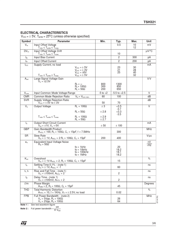
VCC = ± 5V, Tamb = 25oC (unless otherwise specified) Symbol Vio DV io Iib Iio ICC Parameter Input Offset Voltage Tmin ≤ Tamb ≤ Tmax. STMicroelectronics