Download TSH93 Datasheet PDF
STMicroelectronics
TSH93
TSH93 is HIGH SPEED LOW POWER TRIPLE OPERATIONAL AMPLIFIER manufactured by STMicroelectronics.
DESCRIPTION The TSH93 is a triple low power high frequency op-amp, designated for high quality video signal processing. The device offers an excellent speed consumption ratio with 4.5m A per amplifier for 150MHz bandwidth. High slew rate and low noise make it also suitable for high quality audio applications. ORDER CODE Package Part Number TSH93I Temperature Range D -40°C, +125°C - 
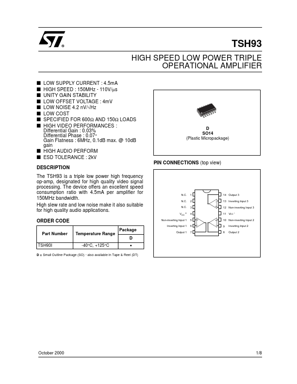
D SO14 (Plastic Micropackage) PIN CONNECTIONS (top view) N.C. N.C. N.C. VCC + Non-inverting Input 1 Inverting Input 1 Output 1 1 2 3 4 5 6 7 + + + 14 Output 3 13 Inverting Input 3 12 Non-inverting Input 3 11 VCC 10 Non-inverting Input 2 9 8 Inverting Input 2 Output 2 D = Small Outline Package (SO) - also available in Tape & Reel (DT) October 2000 1/8 SCHEMATIC DIAGRAM (1/3) V CC+ non inverting input Internal Vref inverting input output Cc VCC- MAXIMUM RATINGS Symbol VCC Vid Vi Toper Tstg Supply Voltage 1) Differential Input Voltage 2) Input Voltage 3) Parameter Value 14 ±5 -0.3 to 12 -40 to +125 -65 to +150 Unit V V V °C °C Operating Free-Air Temperature range Storage Temperature Range 1. All voltages values, except differential voltage are with respect to network ground terminal 2. Differential voltages are the non-inverting input terminal with respect to the inverting input terminal 3. The magnitude of input and output voltages must never exceed VCC+ +0.3V OPERATING CONDITIONS Symbol VCC Vic Supply Voltage mon Mode Input Voltage Range - Parameter Value 7 to 12 VCC +2 to VCC -1 + Unit V V 2/8 ELECTRICAL CHARACTERISTICS VCC+ = 5V, V CC- = -5V, Tamb = 25°C (unless otherwise specified) Symbol Vio Iio Iib ICC CMR SVR Avd Parameter Input Offset Voltage Tmin. ≤ Tamb ≤ Tmax. Input Offset Current Tmin. ≤ Tamb ≤ Tmax. Input Bias Current. Tmin. ≤ Tamb ≤ Tmax. Supply Current (per amplifier, no load) Tmin. ≤ Tamb ≤ Tmax. mon-mode Rejection Ratio Vic = -3V to +4V, Vo = 0V Tmin. ≤ Tamb ≤ Tmax. Supply Voltage Rejection Ratio VCC = ±5V to ±3V Tmin. ≤ Tamb ≤ Tmax Large...