DESCRIPTION
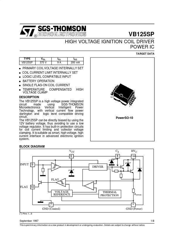
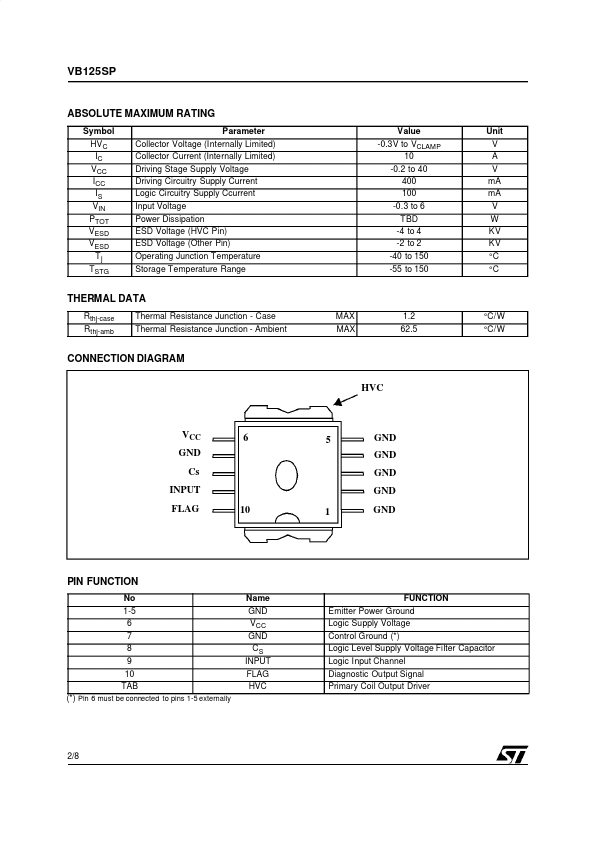
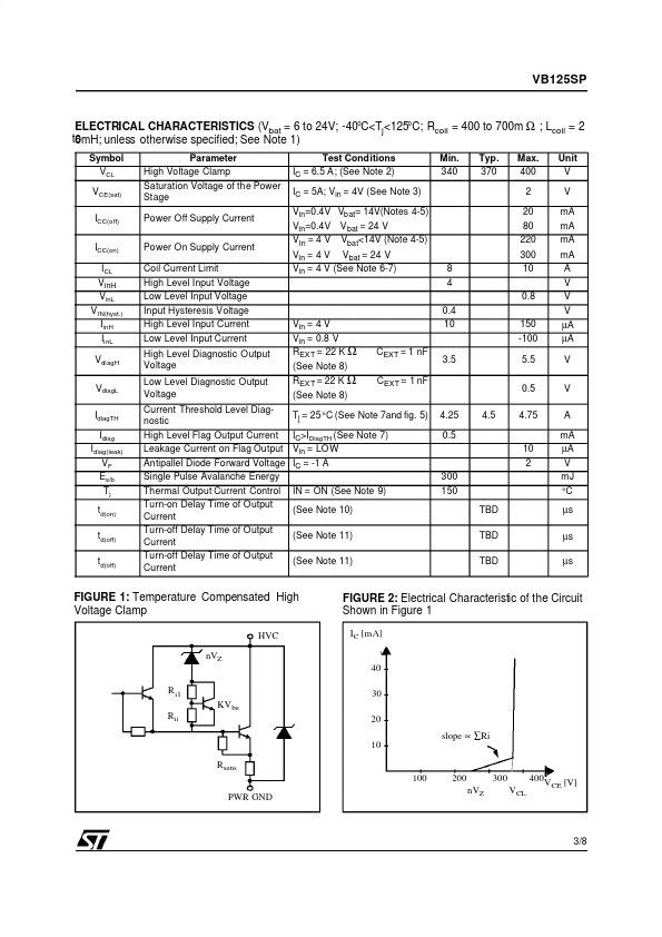
It is suitable as smart, high voltage, high current interface in advanced electronic ignition system. BLOCK DIAGRAM VCC 6 INPUT 9 1 PowerSO-10 CS 8 HVC TAB DRIVER FLAG FLAG 10 VOLTAGE REFERENCE THERMAL PROTECTION RSENSE 7 GND (Control) (*) Pins 1...5 September 1997 * GND (Power) 1/8 This is preliminary information on a new product in development or undergoing evaluation. Details are subject to change without notice. 1 VB125SP ABSOLUTE MAXIMUM RATING Symbol HV C IC VCC ICC IS VIN PTOT VESD VESD Tj TSTG Parameter Collector Voltage (Internally Limited) Collector Current (Internally Limited) Driving Stage Supply Voltage Driving Circuitry Supply Current Logic Circuitry Supply Ccurrent Input Voltage Power Dissipation ESD Voltage (HVC Pin) ESD Voltage (Other Pin) Operating Junction Temperature Storage Temperature Range Value -0.3V to VCLAMP 10 -0.2 to 40 400 100 -0.3 to 6 TBD -4 to 4 -2 to 2 -40 to 150 -55 to 150 Unit V A V mA mA V W KV KV °C °C THERMAL DATA Rthj-case Rthj-amb The... STMicroelectronics