VN05HSP
VN05HSP is HIGH SIDE SMART POWER SOLID STATE RELAY manufactured by STMicroelectronics.
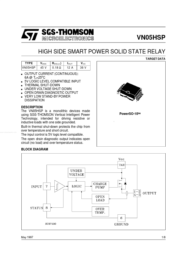
DESCRIPTION
The VN05HSP is a monolithic devices made using SGS-THOMSON Vertical Intelligent Power Technology, intended for driving resistive or inductive loads with one side grounded. Built-in thermal shut-down protects the chip from over temperature and short circuit. The input control is 5V logic level patible. The open drain diagnostic output indicates open circuit (no load) and over temperature status. BLOCK DIAGRAM
Power SO-10™
May 1997
1/8
ABSOLUTE MAXIMUM RATING
Symbol V(BR)DSS I OUT IR I IN VCC VCC -VCC I STAT VESD Pto t Tj T stg ERB Output Current (con t.) Reverse Output Curren t Input Current Supply Voltage (continuou s) Supply Voltage (pulsed) Reverse Supply Voltage Status Current Electrostat ic Discharge (1.5 k Ω, 100 p F) Power Dissipation at T c ≤ 25 C o
Parameter Drain-Source Breakdown Voltage
Value Internally Clamped 12 -12 ± 10 40 60 -4 ± 10 2000 52 -40 to 150 -55 to 150 350
Unit V A A m A V V V m A V W o o
Junction Operating Temperat ure Storage Temperature Power Mos Avalanche Energy
C C m J
CONNECTION DIAGRAMS
CURRENT AND VOLTAGE CONVENTIONS
2/8
THERMAL DATA
R thj-ca se Rt hj-amb Thermal Resistance Junction-case Thermal Resistance Junction-ambient Max Max 2.4 62.5 o o
C/W C/W
ELECTRICAL CHARACTERISTICS (VCC = 9 to 36 V; -40 ≤ Tj ≤ 125 o C unless otherwise specified) POWER
Symbol VCC R on IS VClamp Parameter Supply Voltage On State Resista nce Supply Curren t V CC
- VOUT I OUT = 6 A I OUT = 6 A Off State On State I OUT = 6 A Test Conditions see note 1 Tj = 25 o C T j ≥ 25 o C 40 45 Min. 5.5 Typ. 13 Max. 36 0.18 0.36 50 15 55 Unit V Ω Ω µA m A V
SWITCHING
Symbol t d(on) tr t d( off) tf (di/dt) on (di/dt)of f Vde mag Parameter Turn-on Delay Time Of Output Current Rise Time Of Output Current Test Conditions I OUT = 6 A Resistive Load Input Rise Time < 0.1 µ s T j = 25 o C I OUT = 6 A Resistive Load Input Rise Time < 0.1 µ s T j = 25 o C Min. Typ. 15 30 20 10 0. 5 2 2 4 -7 -4 -2 Max. Unit µs µs µs µs A/ µ s A/ µ s A/ µ s A/ µ...