VN05N
VN05N is HIGH SIDE SMART POWER SOLID STATE RELAY manufactured by STMicroelectronics.
- Part of the VN0 comparator family.
- Part of the VN0 comparator family.
DESCRIPTION
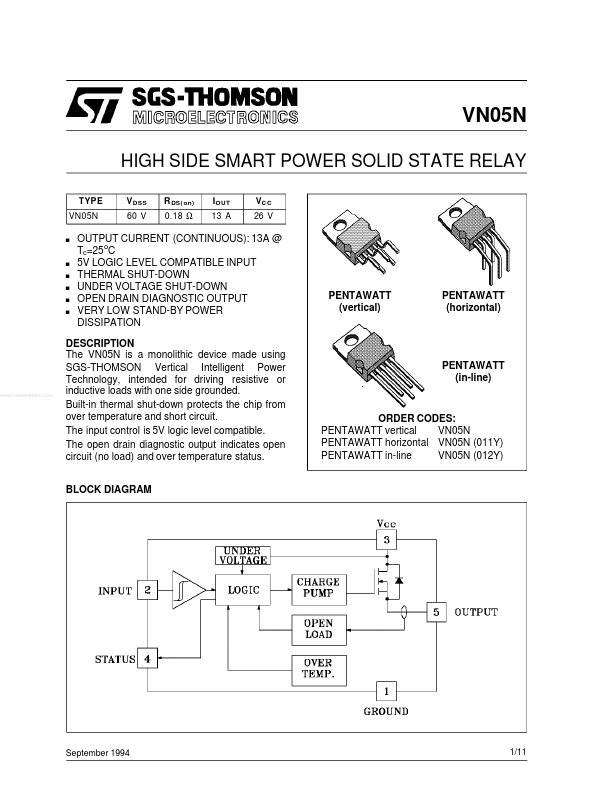
The VN05N is a monolithic device made using SGS-THOMSON Vertical Intelligent Power Technology, intended for driving resistive or inductive loads with one side grounded. Built-in thermal shut-down protects the chip from over temperature and short circuit. The input control is 5V logic level patible. The open drain diagnostic output indicates open circuit (no load) and over temperature status. BLOCK DIAGRAM
PENTAWATT (in-line)
ORDER CODES: PENTAWATT vertical VN05N PENTAWATT horizontal VN05N (011Y) PENTAWATT in-line VN05N (012Y)
September 1994
1/11
ABSOLUTE MAXIMUM RATING
Symbol V( BR)DSS IO UT IR II N -V CC ISTA T VE SD P tot Tj T stg Parameter Drain-Source Breakdown Voltage Output Current (cont.) Reverse Output Current Input Current Reverse Supply Voltage Status Current Electrostatic Discharge (1.5 k Ω , 100 p F) Power Dissipation at T c ≤ 25 C Junction Operating Temperature Storage Temperature o
Value 60 13 -13 ± 10 -4 ± 10 2000 56 -40 to 150 -55 to 150
Unit V A A m A V m A V W o o
CONNECTION DIAGRAM
CURRENT AND VOLTAGE CONVENTIONS
2/11
THERMAL DATA
R thj-cas e Rthj- amb Thermal Resistance Junction-case Thermal Resistance Junction-ambient Max Max 2.2 60 o o
C/W C/W
ELECTRICAL CHARACTERISTICS (VCC = 13 V; -40 ≤ Tj ≤ 125 o C unless otherwise specified) POWER
Symbol VC C R on IS Parameter Supply Voltage On State Resistance Supply Current I OU T = 6 A I OU T = 6 A Off State On State T j = 25 o C T j ≥ 25 o C Test Conditions Min. 7 Typ. Max. 26 0.36 0.18 50 15 Unit V Ω Ω µA m A
SWITCHING
Symbol t d(on) tr t d(off ) tf (di/dt) on (di/dt) off Parameter Test Conditions Min. Typ. 15 30 20 10 0.5 2 2 4 Max. Unit µs µs µs µs A/ µ s A/ µ s A/ µ s A/ µ s
Turn-on Delay Time Of I OU T = 6 A Resistive Load Output Current Input Rise Time < 0.1 µ s T j = 25 o C Rise Time Of Output Current I OU T = 6 A Resistive Load Input Rise Time < 0.1 µ s T j = 25 o C
Turn-off Delay Time Of I OU T = 6 A Resistive Load Output Current Input Rise Time < 0.1 µ s...