STMicroelectronics VND10BSP
The VND10BSP is a monolithic device made using SGS-THOMSON Vertical Intelligent Power Technology, intended for driving resistive or inductive loads with one side grounded. This device has two channels, and a common diagnostic. The status output provides an indication of open load in on state, open load in off state, overtemperature conditions and stuck-on to VCC.| Part No. | VND10BSP |
|---|---|
| Datasheet | VND10BSP Download |
| Manufacturer |  STMicroelectronics |
| Description | ISO HIGH SIDE SMART POWER SOLID STATE RELAY |
| Buy | Stock & Price |
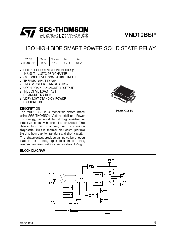
DESCRIPTION
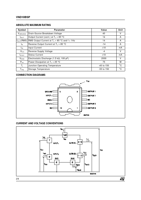
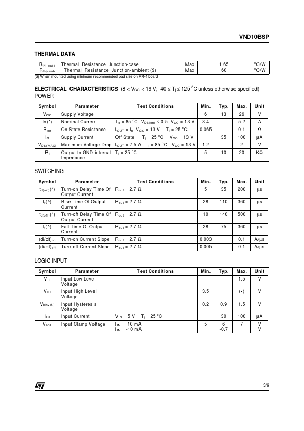
Built-in thermal shut-down protects the chip from over temperature and short circuit. BLOCK DIAGRAM PowerSO-10 March 1998 1/9 VND10BSP ABSOLUTE MAXIMUM RATING Symbol V (BR)DSS I OUT IR I IN -V CC I STAT V ESD P tot Tj T stg Parameter Drain-Source Breakdown Voltage Output Current (cont.) at T c = 85 o C o Value 40 14 14 -14 ± 10 -4 ± 10 2000 75 -40 to 150 -55 to 150 Unit V A A A mA V mA V W o o I OUT (RMS) RMS Output Current at T c = 85 C and f > 1Hz Reverse Output Current at T c = 85 C Input Current Reverse Supply Voltage Status Current Electrostatic Discharge (1.5 k Ω , 100 pF) Power Dissipation at T c = 25 C Junction Operating Temperature Storage Temperature o o C C CONNECTION DIAGRAMS CURRENT AND VOLTAGE CONVENTIONS 2/9 VND10BSP THERMAL DATA R thj-case R thj-amb Thermal Resistance Junction-case Thermal Resistance Junction-ambient ($) Max Max 1.65 60 o o C/W C/W ($) When mounted using minimum recommended pad size on FR-4 boardELECTRICAL CHARACTERISTICS
(8 < VCC < 16 V; -...