W25NM60N
Features
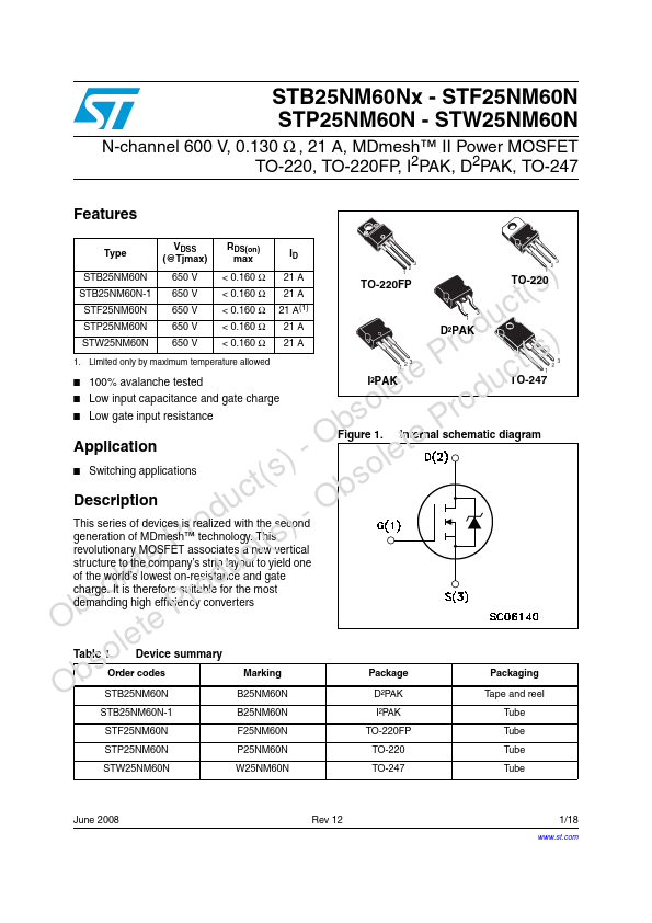
Type
VDSS (@Tjmax)
RDS(on) max
STB25NM60N t(s)STB25NM60N-1 c STF25NM60N u STP25NM60N rod )STW25NM60N
650 V 650 V 650 V 650 V 650 V
< 0.160 Ω < 0.160 Ω < 0.160 Ω < 0.160 Ω < 0.160 Ω
21 A 21 A 21 A(1) 21 A 21 A
P t(s1. Limited only by maximum temperature allowed te c- 100% avalanche tested le du- Low input capacitance and gate charge so ro- Low gate input resistance
- Ob te PApplication ) le- Switching applications ct(s bso Description du
- OThis series of devices is realized with the second ro )generation of MDmesh™ technology. This P t(srevolutionary MOSFET associates a new vertical te cstructure to the pany’s strip layout to yield one le uof the world’s lowest on-resistance and gate dcharge. It is therefore suitable for the most so rodemanding high efficiency converters
3 2 1
TO-220FP
3 1
D²PAK
I²PAK
3 2 1
TO-220
3 2 1
TO-247
Figure 1. Internal schematic diagram
Ob lete PTable 1. Device summary so Order codes
Marking
Ob STB25NM60N
B25NM60N
Package...