STMicroelectronics WH13009
The device is manufactured using high voltage Multi Epitaxial Planar technology for high switching speeds anh high voltage capability. It uses a Hollow Emitter structure to enhance switching speeds.| Part No. | WH13009 |
|---|---|
| Datasheet | WH13009 Download |
| Manufacturer |  STMicroelectronics |
| Description | High voltage fast-switching NPN power transistor |
| Buy | Stock & Price |
FEATURES
● High voltage capability● Low spread of dynamic parameters
● Very high switching speed
APPLICATIONS
● Switching mode power suppliesDESCRIPTION
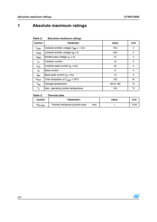
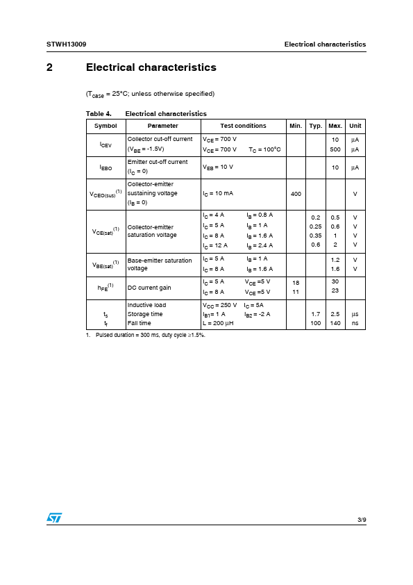
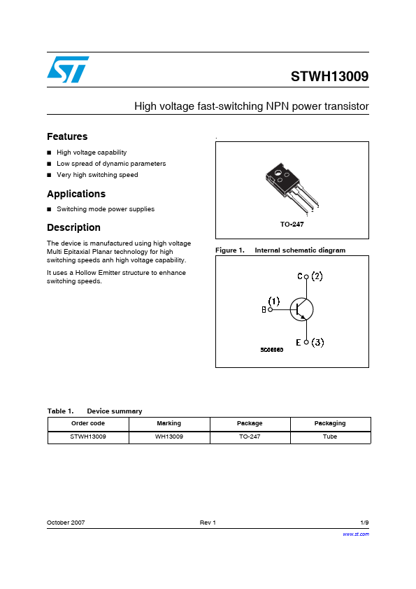
. 3 2 1 TO-247 Figure 1. Internal schematic diagram Table 1. Device summary Order code STWH13009 Marking WH13009 Package TO-247 Packaging Tube October 2007 Rev 1 1/9 9 Absolute maximum ratings 1 Absolute maximum ratings Table 2. Symbol Absolute maximum ratings Parameter VCEV VCEO VEBO IC ICM IB IBM PTOT Tstg TJ Collector-emitter voltage (VBE = -1.5V) Collector-emitter voltage (IB = 0) Emitter-base voltage (IC = 0) Collector current Collector peak current (tp < ms) Base current Base peak current (tp < ms) Total dissipation at Tcase = 25°C Storage temperature Max. operating junction temperature Table 3. Thermal data Symbol Parameters Rthj-case Thermal resistance junction-case __max STWH13009 Value 700 400 12 12 24 6 12 125 -65 to 150 150 Value 1 Unit V V V A A A A W °C °C Unit °C/W 2/9 STWH13009 2 Electrical characteristics Electrical characteristics (Tcase = 25°C; unless otherwise specified) Table 4.