AO2301 Overview
Key Features
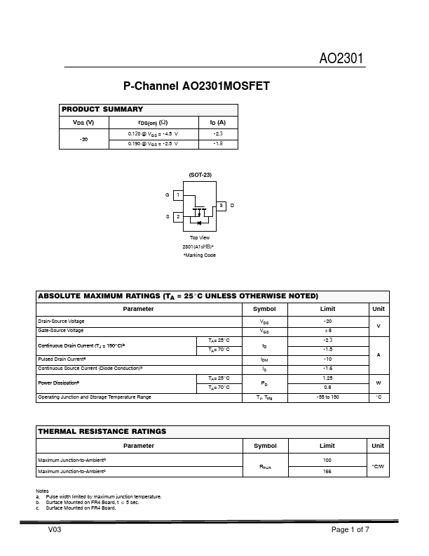
- 20 "8 - 2.3 - 1.5 - 10 - 1.6 1.25 0.8 - 55 to 150
| Part | AO2301 |
|---|---|
| Description | P-Channel MOSFET |
| Category | MOSFET |
| Manufacturer | SZChip |
| Size | 82.50 KB |
| Seller | Inventory | Price Breaks | Buy |
|---|---|---|---|
| Win Source | 15000 | 1250+ : 0.0401 USD 2660+ : 0.0376 USD 4135+ : 0.0363 USD 5920+ : 0.0338 USD |
View Offer |
| RC Electronics | 9072 | 1+ : 0.044 USD 10+ : 0.04 USD 100+ : 0.04 USD 1000+ : 0.04 USD |
View Offer |
| Part Number | Manufacturer | Description |
|---|---|---|
| AO2301 | VBsemi | P-Channel MOSFET |
| AO2302 | HAOHAI | N-Channel Enhancement Mode Field Effect Transistor |
| AO2305 | HAOHAI | P-Channel MOSFET |