STF8233
STF8233 is Dual N-Channel Enhancement Mode Field Effect Transistor manufactured by SamHop Microelectronics.
Green Product
Ver 2.1
S a mHop Microelectronics C orp.
Dual N-Channel Enhancement Mode Field Effect Transistor
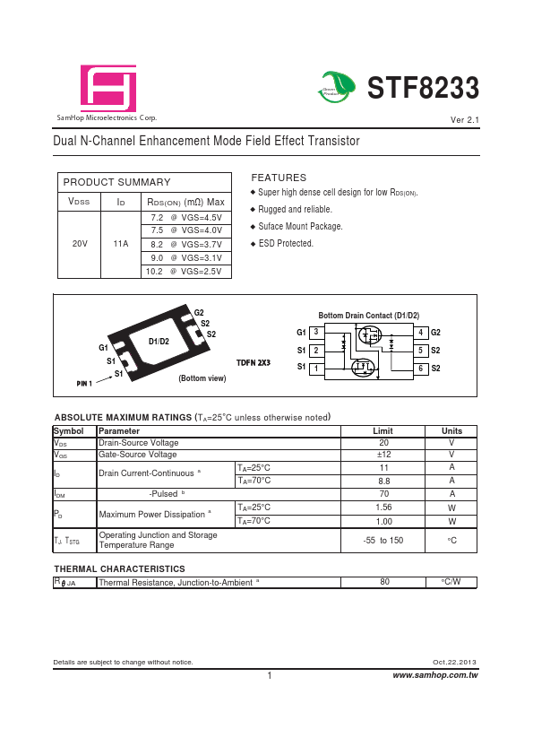
PRODUCT SUMMARY
V DSS ID R DS(ON) (m Ω) Max
7.2 @ VGS=4.5V 7.5 @ VGS=4.0V 20V 11A 8.2 @ VGS=3.7V 9.0 @ VGS=3.1V 10.2 @ VGS=2.5V
Features
Super high dense cell design for low R DS(ON). Rugged and reliable. Suface Mount Package. ESD Protected.
G2 S2 S2 G1 S1 S1
P IN 1
Bottom Drain Contact (D1/D2)
G1 3 S1 2
T DF N 2X3
4 G2 5 6 S2 S2
D1/D2
S1
(Bottom...