Datasheet Summary
S T M4532
S amHop Microelectronics C orp.
Mar.30, 2005 V er1.1
Dual E nhancement Mode Field E ffect Transistor ( N and P Channel)
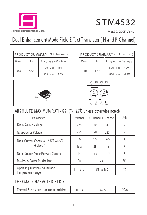
P R ODUC T S UMMAR Y (N-C hannel)
V DS S
30V
P R ODUC T S UMMAR Y (P -C hannel)
V DS S
-30V
5.5A
R DS (ON)
( m W ) Max
-4.5A
R DS (ON)
( m W ) Max
40@ V G S = 10V 50@ V G S = 4.5V
D1
55@ V G S = -10V 85@ V G S = -4.5V
D1
D2
D2
S O-8 1
1 2 3 4
S1
G1 S 2
G2
ABS OLUTE MAXIMUM R ATINGS (T A=25 C unless otherwise noted)
P arameter Drain-S ource Voltage Gate-S ource Voltage Drain C urrent-C ontinuous a @ T J =125 C b -P ulsed Drain-S ource Diode Forward C urrent a Maximum P ower Dissipation a Operating Junction and S torage Temperature...