STS2620A
STS2620A is Dual Enhancement Mode Field Effect Transistor manufactured by SamHop.
S a mHop Microelectronics C orp.
Ver1.2
Dual Enhancement Mode Field Effect Transistor (N and P Channel )
PRODUCT SUMMARY (N-Channel)
V DSS
20V
PRODUCT SUMMARY (P-Channel)
V DSS
-20V
2.5A
R DS(ON) (m Ω) Max
50 @ VGS=4.5V
-2A
R DS(ON) (m Ω) Max
106 @ VGS=-4.5V 198 @ VGS=-2.5V
76 @ VGS=2.5V
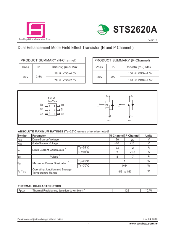
SOT 26 Top View
D1
D2
G1 S2 G2
1 2 3
6 5 4
D1 S1 D2
G1
G2
S1 Nch
S2 P...