K4X51163PC-LG
Overview
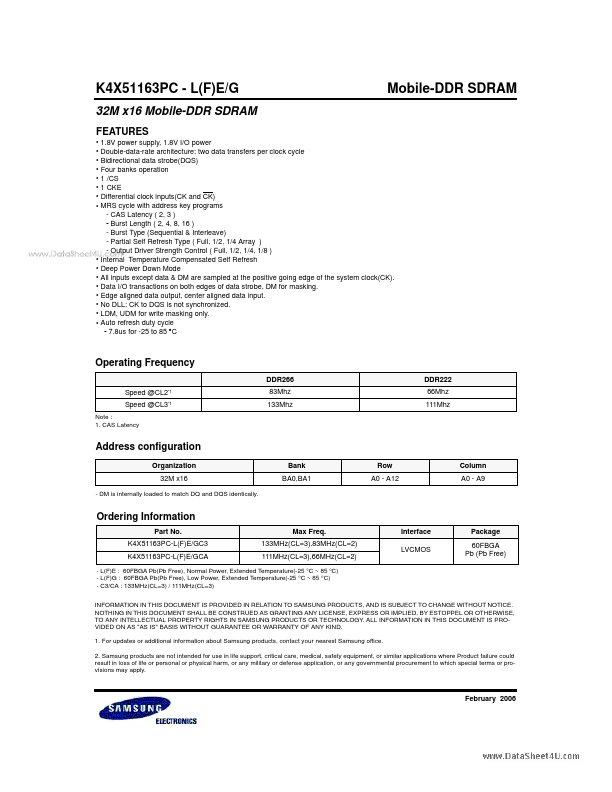
- 1.8V power supply, 1.8V I/O power
- Double-data-rate architecture; two data transfers per clock cycle
- Bidirectional data strobe(DQS)
- Four banks operation
- 1 /CS
- 1 CKE
- Differential clock inputs(CK and CK)
- MRS cycle with address key programs - CAS Latency ( 2, 3 ) - Burst Length ( 2, 4, 8, 16 ) - Burst Type (Sequential & Interleave) - Partial Self Refresh Type ( Full, 1/2, 1/4 Array ) - Output Driver Strength Control ( Full, 1/2, 1/4, 1/8 )
- Internal Temperature Compensated Self Refresh
- Deep Power Down Mode