Samsung semiconductor K7S3236U4C
1Mx36 & 2Mx18 QDR II b4 SRAM
| Part No. | K7S3236U4C |
|---|---|
| Datasheet | K7S3236U4C Download |
| Manufacturer |  Samsung semiconductor |
| Description | 1Mx36 & 2Mx18 QDR II b4 SRAM |
| Buy | Stock & Price |
FEATURES
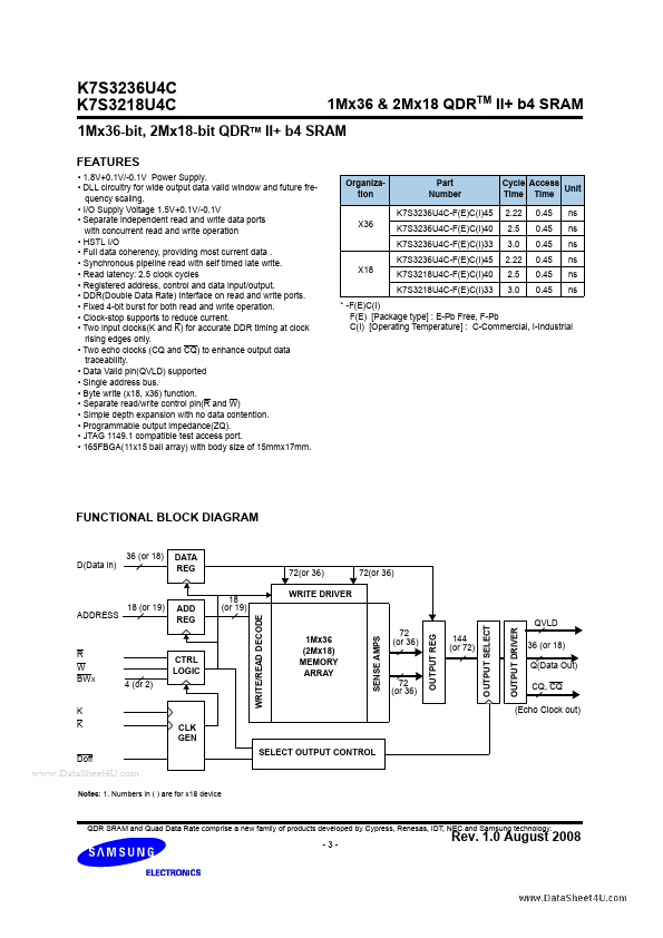
● 1.8V+0.1V/-0.1V Power Supply.● DLL circuitry for wide output data valid window and future frequency scaling.
● I/O Supply Voltage 1.5V+0.1V/-0.1V
● Separate independent read and write data ports with concurrent read and write operation
● HSTL I/O
● Full data coherency, providing most current data .
● Synchronous pipeline read with self timed late write.
● Read latency: 2.5 clock cycles
● Registered address, control and data input/output.
● DDR(Double Data Rate) Interface on read and write ports.
● Fixed 4-bit burst for both read and write operation.
● Clock-stop supports to reduce current.
● Two input clocks(K and K) for accurate DDR timing at clock rising edges only.
● Two echo clocks (CQ and CQ) to enhance output data traceability.
● Data Valid pin(QVLD) supported
● Single address bus.
● Byte write (x18, x36) function.
● Separate read/write control pin(R and W)
● Simple depth expansion with no data contention.
● Programmable output impedance(ZQ).
● JTAG 1149.1 compatible test access port.