Overview: 
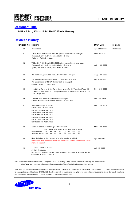
K9F1208Q0A K9F1208D0A K9F1216D0A K9F1208U0A K9F1216U0A
Document Title
64M x 8 Bit , 32M x 16 Bit NAND Flash Memory FLASH MEMORY Revision History Revision No. History 0.0 Initial issue. 0.1 TBGA(K9F12XXX0A-DCB0/DIB0) size information is changed. (before) 9 x 11 /0.8mm pitch , Width 1.0 mm (after ) To Be Decided. 0.2 TBGA(K9F12XXX0A-DCB0/DIB0) size information is changed. (before) 9 x 11 /0.8mm pitch , Width 1.0 mm, to (after) 8.5 x 15 /0.8mm pitch, Width 1.0mm Draft Date
Apr. 25th 2002 May. 9th 2002 Remark
Preliminary July, 10th 2002 0.3 Pin numbering includes TBGA Dummy ball . (Page5) Aug, 10th 2002 0.4 Pin numbering excludes TBGA Dummy ball . (Page5) Pin assignment of TBGA dummy ball is changed. (before) DNU --> (after) N.C Oct, 21th 2002 0.5 1. Add the Rp vs tr ,tf & Rp vs ibusy graph for 1.8V device (Page 43) Nov, 21th 2002 2. Add the data protection Vcc guidence for 1.8V device - below about 1.1V. (Page 44) 0.6 The min. Vcc value 1.8V devices is changed. K9F1208Q0A : Vcc 1.65V~1.95V --> 1.70V~1.95V Mar. 5th 2003 0.7 Pb-free Package is added. K9F1208U0A-FCB0,FIB0 K9F1208Q0A-HCB0,HIB0 K9F1216U0A-HCB0,HIB0 K9F1216U0A-PCB0,PIB0 K9F1216Q0A-HCB0,HIB0 K9F1208U0A-HCB0,HIB0 K9F1208U0A-PCB0,PIB0 Mar. 13rd 2003 0.8 Errata is added.(Front Page)-K9F1208Q0A tWC tWH tWP tRC tREH tRP tREA tCEA Specification 45 15 25 50 15 25 30 45 Relaxed value 60 20 40 60 20 40 40 55 Mar. 17th 2003 0.9 New definition of the number of invalid blocks is added. Apr. 4th 2003 (Minimum 1004 valid blocks are guaranteed for each contiguous 128Mb memory space.) 1.0 1. 2.65V device is added. 2. Note is added. Jul. 4th 2003 (VIL can undershoot to -0.4V and VIH can overshoot to VCC +0.4V for durations of 20 ns or less.