K9K1208U0A-YIB0
K9K1208U0A-YIB0 is 64M x 8 Bit NAND Flash Memory manufactured by Samsung Semiconductor.
description
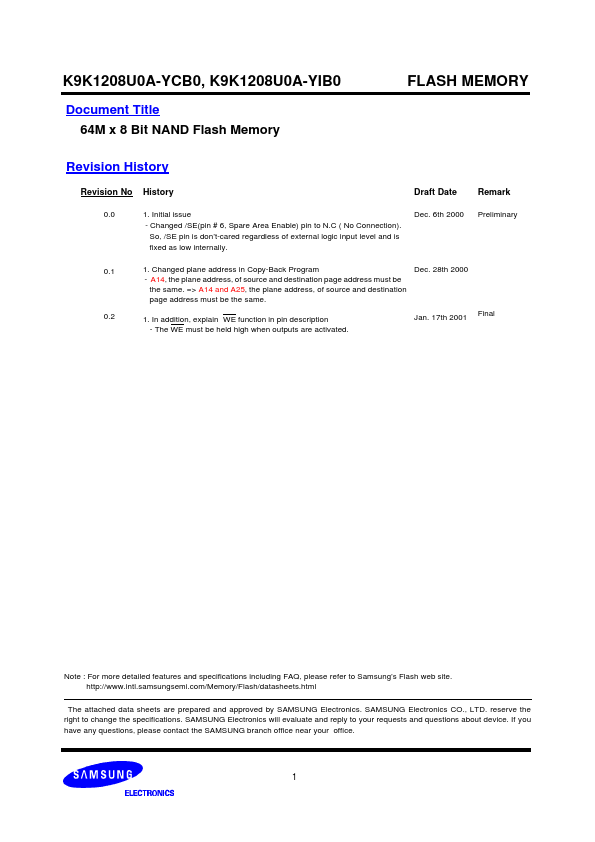
- The WE must be held high when outputs are activated. Jan. 17th 2001 Final
Note : For more detailed features and specifications including FAQ, please refer to Samsung’ s Flash web site. http://.intl.samsungsemi./Memory/Flash/datasheets.html The attached data sheets are prepared and approved by SAMSUNG Electronics. SAMSUNG Electronics CO., LTD. reserve the right to change the specifications. SAMSUNG Electronics will evaluate and reply to your requests and questions about device. If you have any questions, please contact the SAMSUNG branch office near your office.
K9K1208U0A-YCB0, K9K1208U0A-YIB0
FLASH MEMORY
64M x 8 Bit NAND Flash Memory
FEATURES
- Voltage Supply : 2.7V~3.6V
- Organization
- Memory Cell Array : (64M + 2,048K)bit x 8bit
- Data Register : (512 + 16)bit x8bit
- Automatic Program and Erase
- Page Program : (512 + 16)Byte
- Block Erase : (16K + 512)Byte
- 528-Byte Page Read Operation
- Random Access : 10µs(Max.)
- Serial Page Access : 60ns(Min.)
- Fast Write Cycle Time
- Program time : 200µ s(Typ.)
- Block Erase Time : 2ms(Typ.)
- mand/Address/Data Multiplexed I/O Port
- Hardware Data Protection
- Program/Erase Lockout During Power Transitions
- Reliable CMOS Floating-Gate Technology
- Endurance : 100K Program/Erase Cycles
- Data Retention : 10 Years
- mand Register Operation
- Package :
- K9K1208U0A-YCB0/YIB0 : 48
- Pin TSOP I (12 x 20 / 0.5 mm pitch)
GENERAL DESCRIPTION
The K9K1208U0A are a 64M(67,108,864)x8bit NAND Flash Memory with a spare 2,048K(2,097,152)x8bit. Its NAND cell provides the most cost-effective solution for the solid state mass storage market. A program operation programs the 528byte page in typically 200µs and an erase operation can be performed in typically 2ms on a 16K-byte block. Data in the page can be read out at 60ns cycle time per byte. The I/O pins serve as the ports for address and data input/output as well as mand inputs. The on-chip write controller automates all program and erase functions...