K8Q2815UQB Description
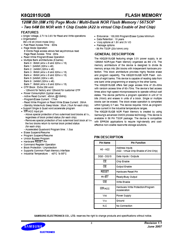
Read While Program/Erase Operation Multiple Bank architectures (8 banks) Bank 0 : 24Mbit (32Kw x 48) The K8Q2815UQB featuring single 3.0V.
K8Q2815UQB Key Features
- Single Voltage, 2.7V to 3.6V for Read and Write operations
- Endurance : 100,000 Program/Erase Cycles Minimum
- Organization
- Data Retention : 10 years
- Vccq options at 1.8V and 3V I/O
- Fast Read Access Time : 60ns
- Package options
- Page Mode Operation 8 Words Page access allows fast asychronous read Page Read Access Time : 20ns
- 56 Pin TSOP (20x14mm) only
- Read While Program/Erase Operation
K8Q2815UQB Applications
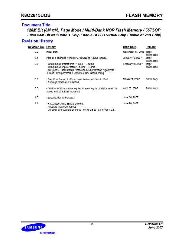
- Samsung Electronics reserves the right to change products or specification without notice
- Two 64M Bit NOR with 1 Chip Enable (A22 is virtual Chip Enable of 2nd Chip)