K9F5608D0C Description
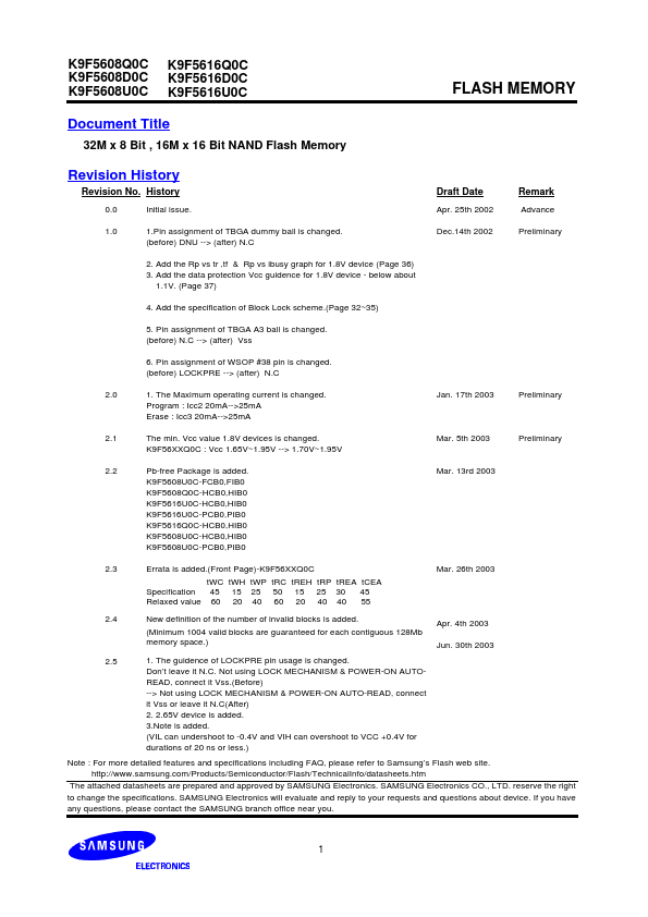
History 0.0 Initial issue. 25th 2002 Remark Advance 1.0 1.Pin assignment of TBGA dummy ball is changed. (before) DNU --> (after) N.C Dec.14th 2002 Preliminary.
K9F5608D0C is NAND Flash Memory manufactured by Samsung Semiconductor.
| Manufacturer | Part Number | Description |
|---|---|---|
| K9F5608D0D | 32M x 8 Bit NAND Flash Memory |
History 0.0 Initial issue. 25th 2002 Remark Advance 1.0 1.Pin assignment of TBGA dummy ball is changed. (before) DNU --> (after) N.C Dec.14th 2002 Preliminary.