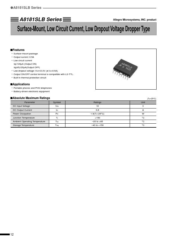
A8181SLB
Overview
- Surface-mount package
- Output current: 0.5A
- Low circuit current Iq≤120µA (Output ON) Iq(off)≤20µA(Output OFF)
- Low dropout voltage: VDIF≤0.3V (at IO=0.5A)
- Output ON/OFF control terminal is compatible with LS-TTL.
- Built-in thermal protection circuit sApplications
- Portable phones and PHS telephones
- Battery-driven electronic equipment sAbsolute Maximum Ratings Parameter DC Input Voltage DC Output Current Power Dissipation Junction Temperature Ambient Operating Temperature Storage Temperature Symbol VIN IO PD Tj Top Tstg Ratings 10 0.6 1.9(TC=25°C) +150 -20 to +85 -40 to +150 Unit V A W °C °C °C (Ta=25°C) 12 qA8181SLB Series sElectrical Characteristics Ratings Parameter Input Voltage Output Voltage Dropout Voltage Line Regulation Load Regulation Temperature Coefficient of Output Voltage Circuit Current Quiescent Circuit Current Control Voltage (Output ON) Control Voltage VC Terminal* Input Current (Output OFF) Symbol typ. VIN VO Conditions VDIF Conditions ∆VOLINE Conditions ∆VOLOAD Conditions ∆VO/∆Ta Conditions Iq Conditions Iq(off) Conditions VO(off) Conditions VC. OL Conditions IC Conditions IC Conditions * Output is OFF when output ON/OFF terminal is open. -1.0 Ta=85°C -0.1 Ta=25°C VIN=10V, Ta=-20 to +85°C 2.4 VIN=10V, Ta=-20 to +85°C IO=0.5A 10 VIN=5.5 to 10V, IO=0A 50 VIN=6V, IO=0 to 0.5A ± 0.5 Tj=-20 to +85°C 92 VIN=10V, IO=0 to 0.5A 10 VIN=10V, IO=0A, VC=0.4V 4.85 5.00 VIN=5.5 to 10V, IO=0 to 0.5A, Ta=-20 to +85°C A8181SLB min. (Ta=25°C unless otherwise specified) Unit max. 10 5.15 0.3 30 100 ± 1.0 120 20 V V V mV mV mV/°C µA µA V 0.4 +0.1 +1.0 V µA µA sOutline Drawing (unit: mm)
- 10/10.50 16 15 14 13 12 11 10 9
- 23/0.32 0° TO 8° a. Part Number b. Lot Number q w e r t y u i NC NC NC GND GND VC VIN VIN o !00 !11 !2 !3 !