FKI07117
Features
- V(BR)DSS --------------------------------- 75 V (ID = 100 µA)
- ID ---------------------------------------------------------- 42 A
- RDS(ON) ----------9.7 mΩ max. (VGS = 10 V, ID = 31.2 A)
- Qg------25.0 n C (VGS = 4.5 V, VDS = 38 V, ID = 31.2 A)
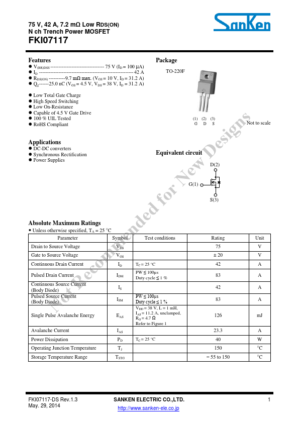
Package
TO-220F
- Low Total Gate Charge
- High Speed Switching
- Low On-Resistance
- Capable of 4.5 V Gate Drive
- 100 % UIL Tested
- Ro HS pliant
Applications
- DC-DC converters
- Synchronous Rectification
(1) (2) (3) s G D S Design Equivalent circuit
Not to scale or New
- Power Supplies
D(2) G(1)
S(3) ed f Absolute Maximum Ratings d
- Unless otherwise specified, TA = 25 °C n Parameter
Symbol e Drain to Source Voltage
VDS m Gate to Source Voltage
VGS m Continuous Drain Current
ID co Pulsed Drain Current
IDM e Continuous Source Current R (Body Diode)
IS t Pulsed Source Current o (Body Diode)
N Single Pulse Avalanche Energy
Test conditions
TC = 25 °C PW ≤ 100µs Duty cycle ≤ 1 %
PW ≤ 100µs Duty cycle...