Sanken SLA5024
P-channel General purpose
| Part No. | SLA5024 |
|---|---|
| Datasheet | SLA5024 Download |
| Manufacturer |  Sanken |
| Description | P-channel General purpose |
| Buy | Stock & Price |
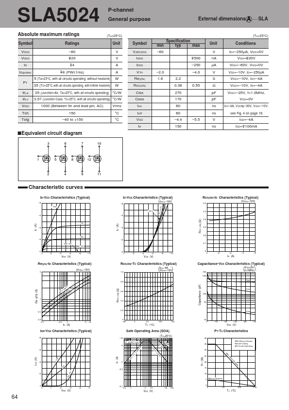
SLA5024 Absolute maximum ratings Symbol VDSS VGSS ID ID(pulse) PT Ratings –60 20 4 8 (PW≤1ms) P-channel General purpose (Ta=25°C) External dimensions A
●●● SLA (Ta=25°C) Unit V V A A W W Symbol V(BR)DSS IGSS IDSS VTH Re(yfs) RDS(ON) Ciss Coss ton toff VSD trr Specification min typ max –60 500 –250 –2.0 1.6 2.2 0.38 270 170 60 60 –4.4 150 –5.5 0.55 –4.0 Unit V nA Conditions ID=–250µA, VGS=0V VGS= 20V VDS=–60V, VGS=0V VDS=–10V, ID=–250µA VDS=–10V, ID=–4A VGS=–10V, ID=–4A VDS=–25V, f=1.0MHz, VGS=0V ID=–4A, VDD –30V, VGS=–10V, see Fig. 4 on page 16. ISD=–4A ISD= 100mA µA V S Ω pF pF ns ns V ns 5 (Ta=25°C, with all circuits operating, without heatsink) 35 (Tc=25°C,with all circuits operating, with infinite heatsink) θ j-a θ j-c VISO Tch Tstg 25 (Junction-Air, Ta=25°C, with all circuits operating) °C/W 3.57 (Junction-Case, Tc=25°C, with all circuits operating) °C/W 1000 (Between fin and lead pin, AC) 150 –40 to +150 Vrms °C °C sEquivalent circuit diagram 3 6 7 10 1 5 8 12 2 4 9 11 Characteri...
●●● SLA (Ta=25°C) Unit V V A A W W Symbol V(BR)DSS IGSS IDSS VTH Re(yfs) RDS(ON) Ciss Coss ton toff VSD trr Specification min typ max –60 500 –250 –2.0 1.6 2.2 0.38 270 170 60 60 –4.4 150 –5.5 0.55 –4.0 Unit V nA Conditions ID=–250µA, VGS=0V VGS= 20V VDS=–60V, VGS=0V VDS=–10V, ID=–250µA VDS=–10V, ID=–4A VGS=–10V, ID=–4A VDS=–25V, f=1.0MHz, VGS=0V ID=–4A, VDD –30V, VGS=–10V, see Fig. 4 on page 16. ISD=–4A ISD= 100mA µA V S Ω pF pF ns ns V ns 5 (Ta=25°C, with all circuits operating, without heatsink) 35 (Tc=25°C,with all circuits operating, with infinite heatsink) θ j-a θ j-c VISO Tch Tstg 25 (Junction-Air, Ta=25°C, with all circuits operating) °C/W 3.57 (Junction-Case, Tc=25°C, with all circuits operating) °C/W 1000 (Between fin and lead pin, AC) 150 –40 to +150 Vrms °C °C sEquivalent circuit diagram 3 6 7 10 1 5 8 12 2 4 9 11 Characteri...