2SJ406
Overview
- Low ON-state resistance.
- Very high-speed switching.
- Low-voltage dreve.
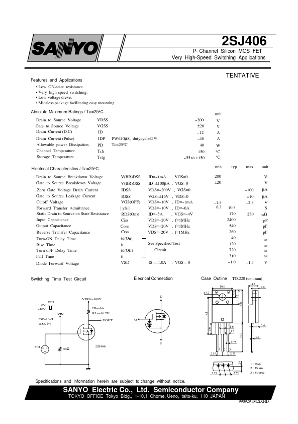
- Micaless package facilitating easy mounting. Absolute Maximum Ratings / Ta=25°C Drain to Source Voltage Gate to Source Voltage Drain Current (D.C) Drain Current (Pulse) Allowable power Dissipation Channel Temperature Storage Temperature VDSS VGSS ID PW≤10µS, dutycycle≤1% IDP Tc=25°C PD Tch Tstg --200 ±20 --12 --48 40 150 --55 to +150 unit V V A A W °C °C min V(BR)DSS V(BR)GSS IDSS IGSS VGS(OFF) | yfs | RDS(On)1 Ciss Coss Crss td(On) tr td(Off) tf VSD ID=--1mA , VGS=0 ID=±100µA , VGS=0 VDS=--200V , VGS=0 VGS=±16V VDS=--10V VDS=--10V ID=--5A VDS=--20V VDS=--20V VDS=--20V , , , , , , , VDS=0 ID=--1mA ID=--6A VGS=--4V f=1MHz f=1MHz f=1MHz --1.5 6.3 --200 ±20 --100 ±10 --2.5 10.5 170 2400 540 260 40 120 720 310 --1.0 230 typ max unit V V µA µA V S mΩ pF pF pF ns ns ns ns --1.5 V