2SK715
Features
- Adoption of FBET process.
- Large yfs.
- Small Ciss.
- Very low noise figure.
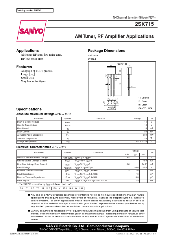
0.4 0.5
1.8 15.0
1 2 1.3
3 1.3
Specifications
Absolute Maximum Ratings at Ta = 25˚C
Parameter Drain-to-Source Voltage Gate-to-Drain Voltage Gate Current Drain Current Allowable Power Dissipation Junction Temperature Storage Temperature Symbol VDSS VGDS IG ID PD Tj Tstg Conditions
3.0 3.8nom
1 : Source 2 : Gate 3 : Drain SANYO : SPA
Ratings 15
- 15 10 50 300 125
- 55 to +125
Unit V V m A m A m W ˚C ˚C
Electrical Characteristics at Ta = 25˚C
Parameter Gate-to-Drain Breakdown Voltage Gate-to-Source Leakage Current Zero-Gate Voltage Drain Current Cutoff Voltage Forward Transfer Admittance Input Capacitance Reverse Transfer Capacitance Noise Figure Symbol V(BR)GDS IG=- 10µA, VDS=0 IGSS VGS=- 10V, VDS=0 IDSS- VGS(off) | yfs | Ciss Crss NF VDS=5V, VGS=0 VDS=5V, ID=100µA VDS=5V, VGS=0, f=1k Hz VDS=5V, VGS=0, f=1k Hz VDS=5V, VGS=0, f=1k Hz VDS=5V, Rg=1kΩ, ID=1m A, f=1k Hz...