LC7930N
LC7930N is LCD Drivers manufactured by SANYO.
Ordering number: EN2778C
CMOS LSI
LC7930N, 7930NW LCD Drivers
Overview
The LC7930N, 7930NW are CMOS LSIs which incorporate 20-bit shift register, latch, and two sets of 20 LCD drivers. They also have two switching pins: one of them (channel 2) can be used as a scan-line driver (back plate) and the other (channel 1) as a segment driver. They are optimal for LCD interface with microcontroller (4 or 8 bits) or dot matrix controller circuit incorporating character generator.
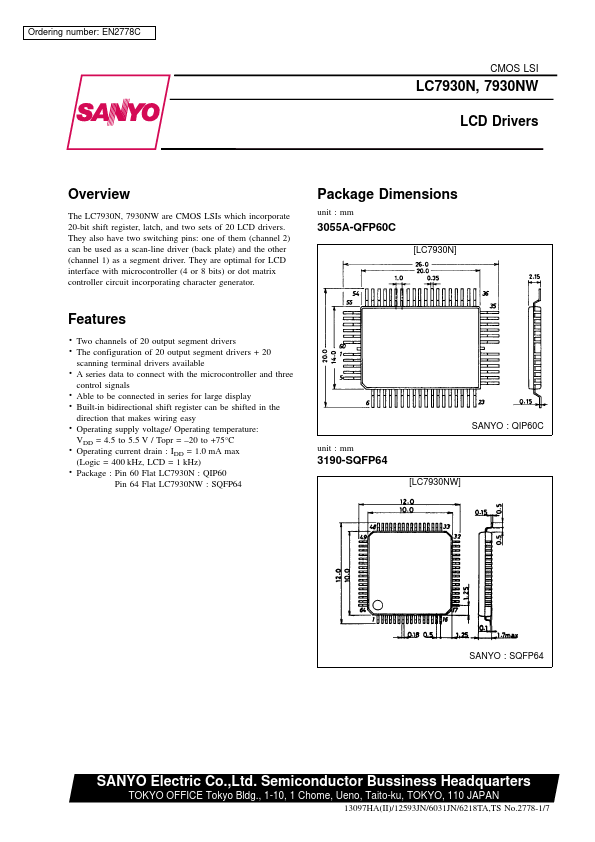
Package Dimensions unit : mm
3055A-QFP60C
[LC7930N]
Features
. Two channels of 20 output segment drivers . The configuration of 20 output segment drivers + 20 terminal drivers available . scanning A series data to connect with the microcontroller and three signals . control Able to be connected in series for large display . Built-in bidirectional shift register can be shifted in the that makes wiring easy . direction Operating supply voltage/ Operating temperature: = 4.5 to 5.5 V / Topr =
- 20 to +75°C .V Operating current drain : I = 1.0 m A max (Logic = 400 k Hz, LCD = 1 k Hz) . Package : Pin 60 Flat LC7930N : QIP60
DD DD
SANYO : QIP60C unit : mm
3190-SQFP64
[LC7930NW]
Pin 64 Flat LC7930NW : SQFP64
SANYO : SQFP64
SANYO Electric Co.,Ltd. Semiconductor Bussiness Headquarters
TOKYO OFFICE Tokyo Bldg., 1-10, 1 Chome, Ueno, Taito-ku, TOKYO, 110 JAPAN
13097HA(II)/12593JN/6031JN/6218TA,TS No.2778-1/7
LC7930N, 7930NW
Specifications...