Datasheet Summary
Ordering number : EN4346B
CMOS LSI
Dot Matrix LCD Driver
Overview
The LC79400D is a large-scale dot matrix LCD segment driver LSI. Display data transferred from the controller (4-bit parallel format) is processed through 80-bit latching and a LCD drive signal is generated. The LC79400D can be used in conjunction with mon driver LC7943D (QIP80D) as well as LC79430D (QIP100D) and LC79431D (QIP100D) to drive a widescreen LCD panel.
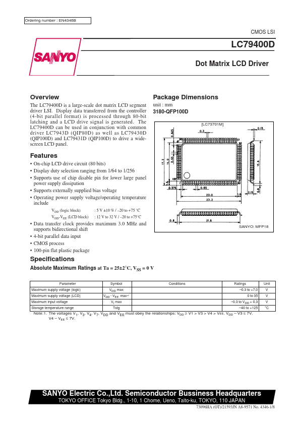
Package Dimensions unit : mm 3180-QFP100D
[LC73701M]
Features
- On-chip LCD drive circuit (80 bits)
- Display duty selection ranging from 1/64 to 1/256
- Supports use of chip disable pin for lower large panel power supply dissipation
- Supports...