Datasheet4U Logo Datasheet4U.com

LV5254LG - Inverting Charge Pump Regulator IC

Description

Outputs a fixed voltage of -2.8V determined by an internal resistor.

Outputs a voltage that is -1 times the voltage VS input to the VS pin.

Outputs a voltage determined by an external resistor and the external reference voltage.

Features

  • with the charge pump sub-driver (soft start). (5) Switch to the.

📥 Download Datasheet

Other Datasheets by Sanyo Semicon Device

Full PDF Text Transcription

Click to expand full text
www.DataSheet.co.kr 
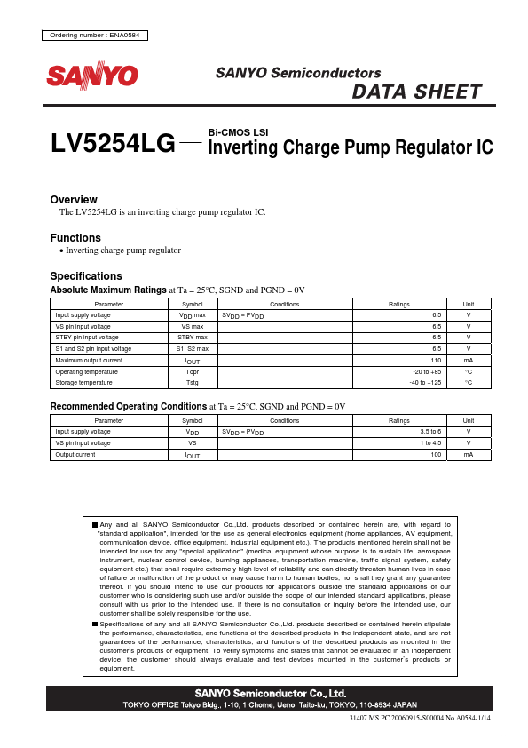
Ordering number : ENA0584 LV5254LG Overview Bi-CMOS LSI Inverting Charge Pump Regulator IC The LV5254LG is an inverting charge pump regulator IC. Functions • Inverting charge pump regulator
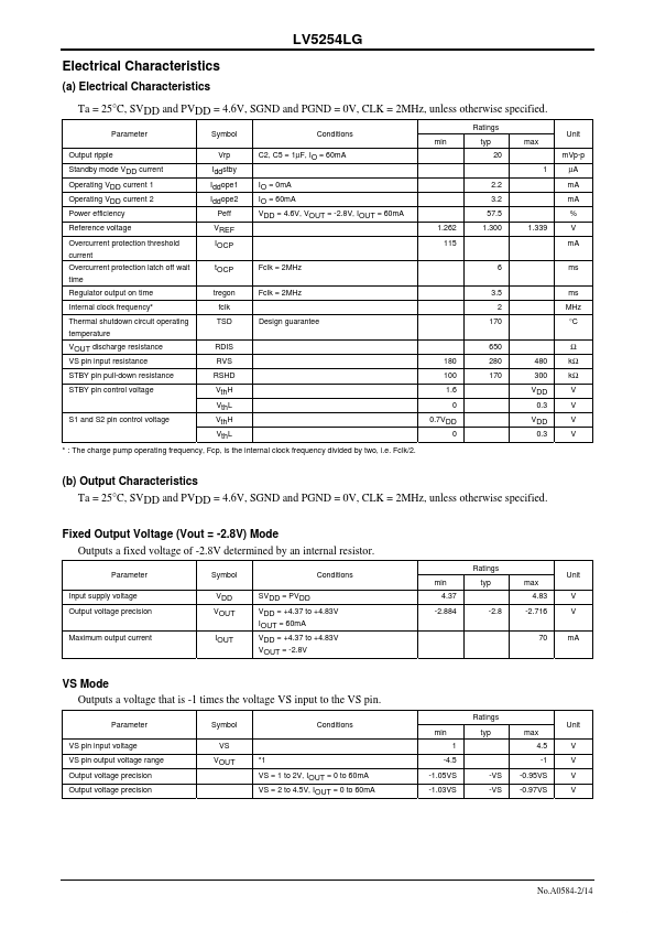
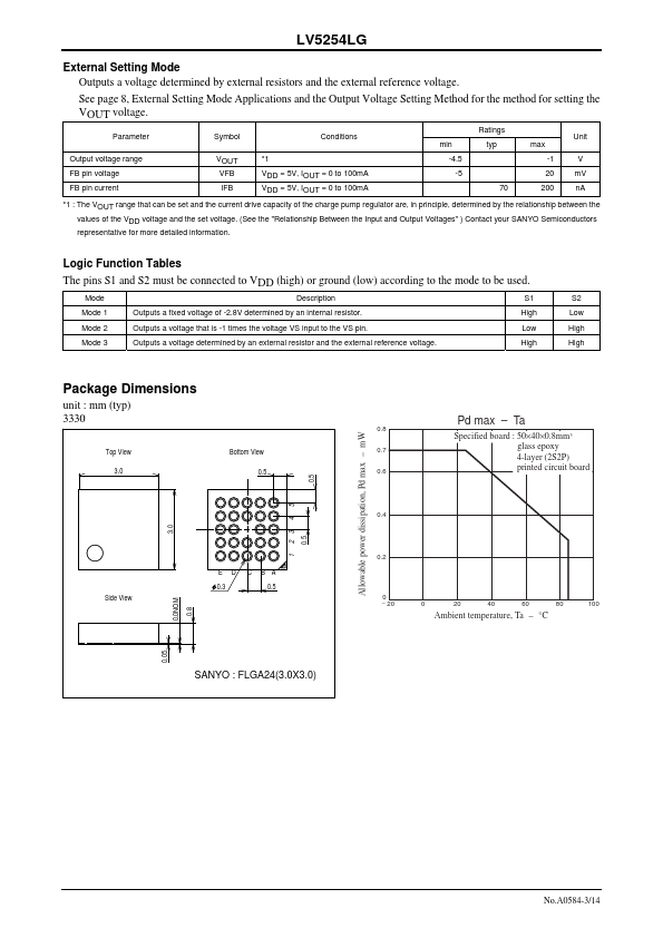
 Specifications Absolute Maximum Ratings at Ta = 25°C, SGND and PGND = 0V Parameter Input supply voltage VS pin input voltage STBY pin input voltage S1 and S2 pin input voltage Maximum output current Operating temperature Storage temperature Symbol VDD max VS max STBY max S1, S2 max IOUT Topr Tstg SVDD = PVDD Conditions Ratings 6.5 6.5 6.5 6.5 110 -20 to +85 -40 to +125 Unit V V V V mA °C °C Recommended Operating Conditions at Ta = 25°C, SGND and PGND = 0V Parameter Input supply voltage VS pin input voltage Output current Symbol VDD VS IOUT SVDD = PVDD Conditions Ratings 3.
Published: |