Datasheet4U.com
🌙
K3255 Datasheet | SANYO
Part:
K3255
Description:
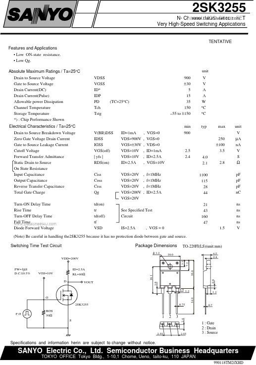
2SK3255
Manufacturer:
SANYO
Size:
38.97 KB
K3255 Datasheet (PDF) Download
SANYO
K3255
Key Features
and Applications
Low ON-state resistance
×
Close