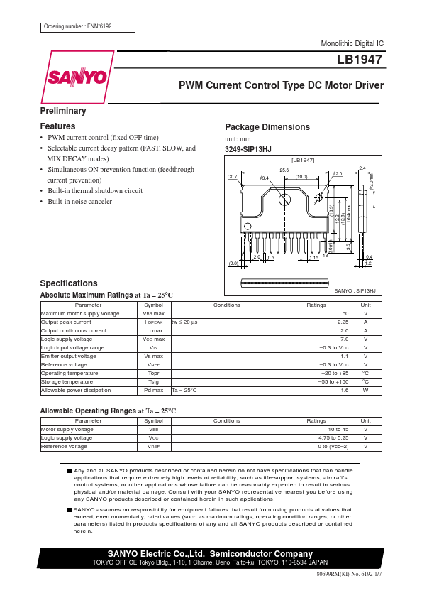
Description
Pin number 1 3 2 4 5 8 9 Pin name OUTA
OUTA E VI ST IN1 IN2 Equivalent circuit Output pin Sense voltage control pin VI High : sense voltage is 2/5 of VREF Low : sense voltage is 1/5 of VREF ST High : circuit operation ON Low : standby mode IN1 High : rotation mode Low : brake mode IN2 High
Features
- PWM current control (fixed OFF time).
- Selectable current decay pattern (FAST, SLOW, and MIX DECAY modes).
- Simultaneous ON prevention function (feedthrough current prevention).
- Built-in thermal shutdown circuit.
- Built-in noise canceler
Package Dimensions
unit: mm 3249-SIP13HJ
[LB1947]
25.6 C0.7
φ 3.4 φ 2.0
2.4
(10.0)
2.0min
1 (0.8)
2.0
0.5
1.15 13
3.5
(13.9) 12.2 (12.8) 16.4max
0.4 1.2
Specifications
Absolute Maximum Ratings at Ta = 25°C
P.