Datasheet4U.com
🌙
LC3564RT-10LV Datasheet | SANYO
Part:
LC3564RT-10LV
Description:
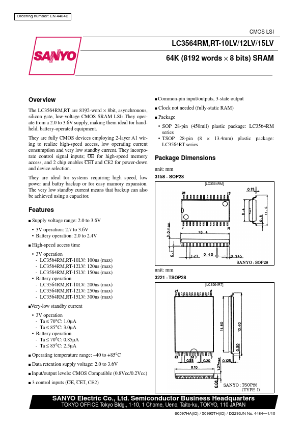
64K (8192 words x 8 bits) SRAM
Manufacturer:
SANYO
Size:
442.22 KB
LC3564RT-10LV Datasheet (PDF) Download
SANYO
LC3564RT-10LV
Key Features
3V operation: 2.7 to 3.6V
Battery operation: 2.0 to 2.4V
3V operation - Ta ≤ 70°C: 1.0µA - Ta ≤ 85°C: 3.0µA
Battery operation - Ta ≤ 70°C: 0.85µA - Ta ≤ 85°C: 2.5µA
×
Close