LC378000RP Datasheet Text
Ordering number : EN- 5793
CMOS IC
LC378000RP
Internally Synchronized Silicon Gate 8M (1,048,576word × 8-bit, 524,288-word × 16-bit) Mask ROM
Preliminary Overview
The LC378000RP is an 8-Mbit mask ROM that can be switched between byte mode, which provides an 8-bit × 1,048,576-word structure, and word mode, which provides a 16-bit × 524,288-word structure. Since this device operates over the wide supply voltage range of 2.6 to 5.5 V and achieves access times (tAA) of 100 ns (at VCC = 4.5 to 5.5 V) and 200 ns (at VCC = 2.6 to 5.5 V), it can be used in a wide range of systems, from 5-V systems requiring high-speed access to 3-V battery operated systems.
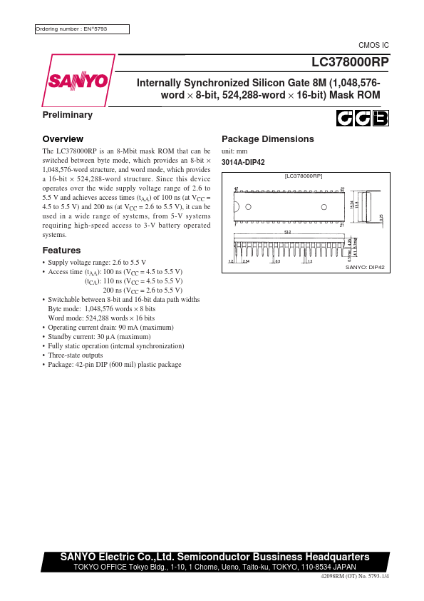
Package Dimensions unit: mm 3014A-DIP42
[LC378000RP]
Features
- Supply voltage range: 2.6 to 5.5 V
- Access time (tAA): 100 ns (VCC = 4.5 to 5.5 V) (tCA): 110 ns (VCC = 4.5 to 5.5 V) 200 ns (VCC = 2.6 to 5.5 V)
- Switchable between 8-bit and 16-bit data path widths Byte mode: 1,048,576 words × 8 bits Word mode: 524,288 words × 16 bits
- Operating current drain: 90 mA (maximum)
- Standby current: 30 µA (maximum)
- Fully static operation (internal synchronization)
- Three-state outputs
- Package: 42-pin DIP (600 mil) plastic package
SANYO: DIP42
SANYO Electric Co.,Ltd. Semiconductor Bussiness Headquarters
TOKYO OFFICE Tokyo Bldg., 1-10, 1 Chome, Ueno, Taito-ku, TOKYO, 110-8534 JAPAN
42098RM (OT) No. 5793-1/4
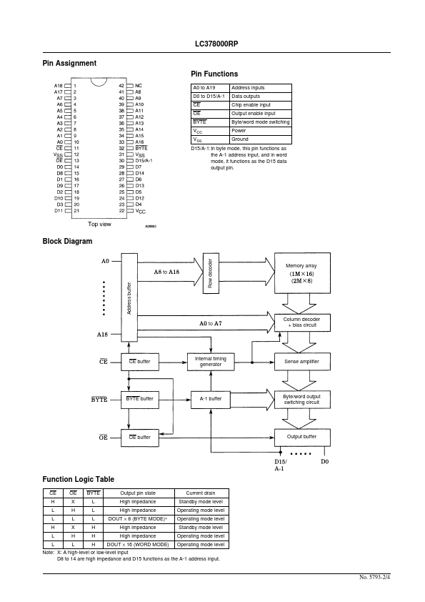
LC378000RP Pin Assignment Pin Functions
A0 to A19 D0 to D15/A-1 CE OE BYTE VCC VSS Address inputs Data outputs Chip enable input Output enable input Byte/word mode switching Power Ground
D15/A-1:In byte mode, this pin functions as the A-1 address input, and in word mode, it functions as the D15 data output pin.
Block Diagram
Row decoder
Memory array
Address buffer
Column decoder + bias circuit
CE...