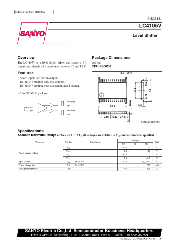
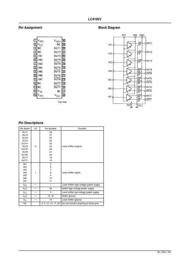
Datasheet4U Logo Datasheet4U.com

LC4105V - Level Shifter

Description

Pin Name OUT1 OUT2 OUT3 OUT4 OUT4 OUT5 OUT5 OUT6 OUT6 OUT7 OUT7 IN1 IN2 IN3 IN4 IN5 IN6 IN7 VDD VDD1 VCC VSS1 VSS NC I/O Pin Number 28 27 26 25 24 23 22 21 20 19 18 5 6 7 8 9 10 11 1 30 2 15, 16 14 3, 4, 12, 13, 17, 29 Function O Level shifter outputs I Level shifter inputs

Features

  • Seven inputs and eleven outputs IN1 to IN3 produce only true outputs. IN4 to IN7 produce both true and inverted outputs.
  • Slim SSOP-30 package SANYO: SSOP30 Specifications Absolute Maximum Ratings at Ta = 25°C ± 2°C, all voltages are relative to VSS, unless otherwise specified Parameter Symbol VDD Power supply voltage VDD1 VCC VSS1 Input voltage Power dissipation Storage temperature VIN Pd Tstg IN1 to IN7 Ta ≤ 75°C.
  • 55 Conditions Ratings min.
  • 0.3.
  • 0.3.

📥 Download Datasheet

Datasheet preview – LC4105V

Datasheet Details

Part number LC4105V
Manufacturer Sanyo
File Size 66.13 KB
Description Level Shifter
Datasheet download datasheet LC4105V Datasheet
Additional preview pages of the LC4105V datasheet.
Other Datasheets by Sanyo

Full PDF Text Transcription

Click to expand full text
Ordering number : 
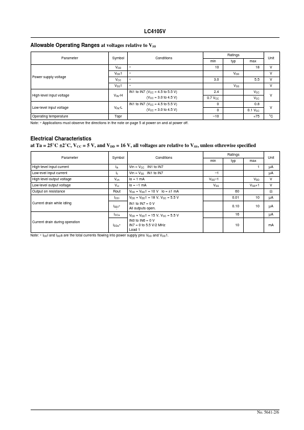
EN5641A CMOS LSI LC4105V Level Shifter Overview The LC4105V is a level shifter driver that converts 5-V signals into signals with amplitudes between 10 and 18 V. Package Dimensions unit: mm 3191-SSOP30 [LC4105V] Features • Seven inputs and eleven outputs IN1 to IN3 produce only true outputs. IN4 to IN7 produce both true and inverted outputs. • Slim SSOP-30 package SANYO: SSOP30 Specifications Absolute Maximum Ratings at Ta = 25°C ± 2°C, all voltages are relative to VSS, unless otherwise specified Parameter Symbol VDD Power supply voltage VDD1 VCC VSS1 Input voltage Power dissipation Storage temperature VIN Pd Tstg IN1 to IN7 Ta ≤ 75°C –55 Conditions Ratings min –0.3 –0.3 –0.3 –0.3 –0.5 typ max 20 20 7 +0.3 VCC +0.5 200 +125 Unit V V V V V mW °C SANYO Electric Co.
Published: |