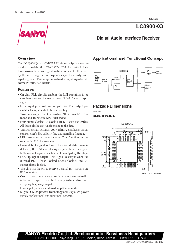
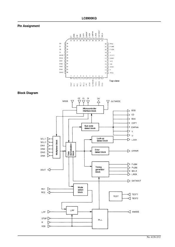
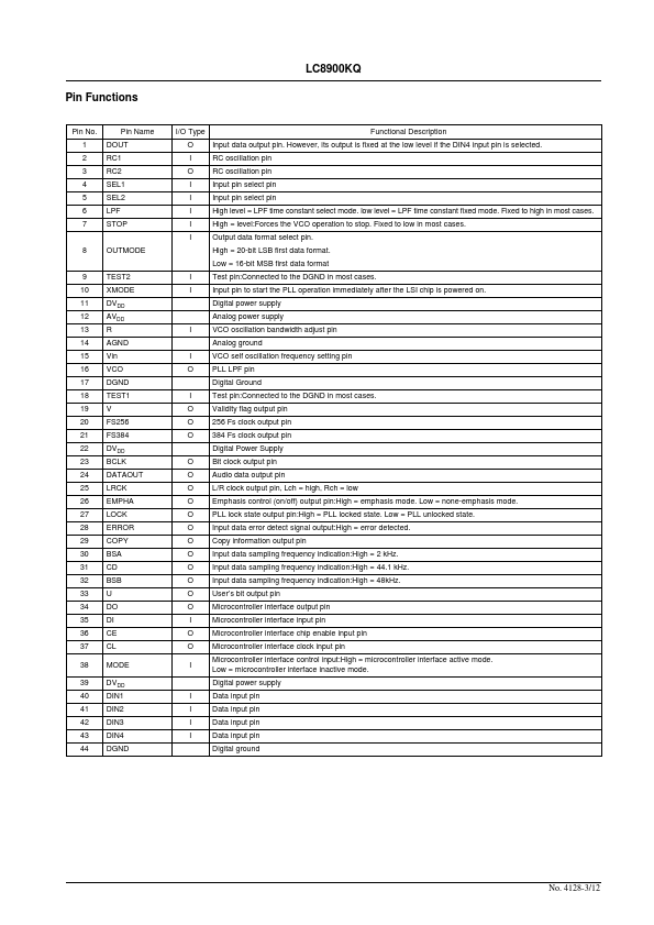
LC8900KQ Description
However, its output is fixed at the low level if the DIN4 input pin is selected. RC oscillation pin RC oscillation pin Input pin select pin Input pin select pin High level = LPF time constant select mode. low level = LPF time constant fixed mode.
LC8900KQ Key Features
- On-chip PLL circuit: enables the LSI operation to be synchronous to the transmitted EIAJ format input signals
- Four input pins and one output pin: The output pin enables the input data to be sent as they are
- Two data output function modes: 20-bit data LSB first mode and 16-bit data MSB first mode
- Four output clocks: Bit clock, LRCK, 384Fs and 256Fs. All these clocks are synchronized to the data
- Various signal outputs: copy inhibit, emphasis on:off control, user’s bit, validity flag and sampling frequency
- LPF time constant select mode: This function can be used in the PLL lock-up state
- Error detect signal output: If an input data error is detected, this LSI circuit chip outputs the error signal. In this
- Lock-up signal output: This signal is output when the internal PLL (Phase Locked Loop) block of the LSI circuit chip is
- The chip has the pin to receive a signal for stopping the PLL operation
- Control and processing mode via microcontroller interface: input pin select, copy information and sampling frequency out