Datasheet Summary
Ordering number : EN- 4852B
CMOS LSI
CD-ROM Error Correction LSI with Built-In SCSI Interface
Preliminary Overview
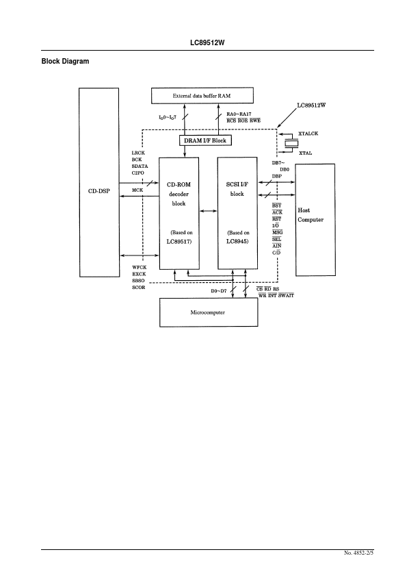
The LC89512W integrates a real-time error correction circuit and a SCSI interface in a single chip.
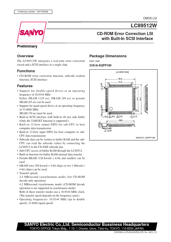
Package Dimensions unit: mm 3181A-SQFP100
[LC89512W]
Functions
- CD-ROM error correction function, subcode readout function, SCSI interface
Features
- Support for double-speed drives at an operating frequency of 16.9344 MHz Either SRAM (120 ns), DRAM (80 ns) or pseudo SRAM (85 ns) can be used.
- Support for quad-speed drives at an operating frequency of 33.8688 MHz SRAM (70 ns) must be used.
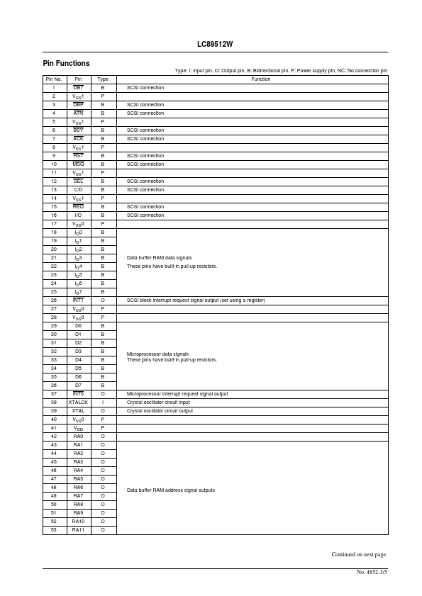
- Built-in SCSI interface with built-in 48 mA sink buffer (Only the TARGET...