Datasheet Summary
Ordering number: EN3202A
LC8991 NTSC CCD 1H Delay Line
Overview
The Sanyo LC8991 is a 1H delay line for NTSC television systems.
. Sample-and-hold circuit
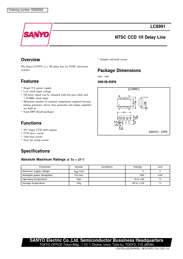
Package Dimensions unit : mm
Features
3001B-DIP8
[LC8991]
. Single 9 V power supply . Low clock input voltage . 1H delay signal can be obtained with low-pass filter and MHz clock input . 7.16 Minimum number of external ponents required because . timing generator, driver, bias generator and output amplifier are built in 8-pin DIP (Small package)
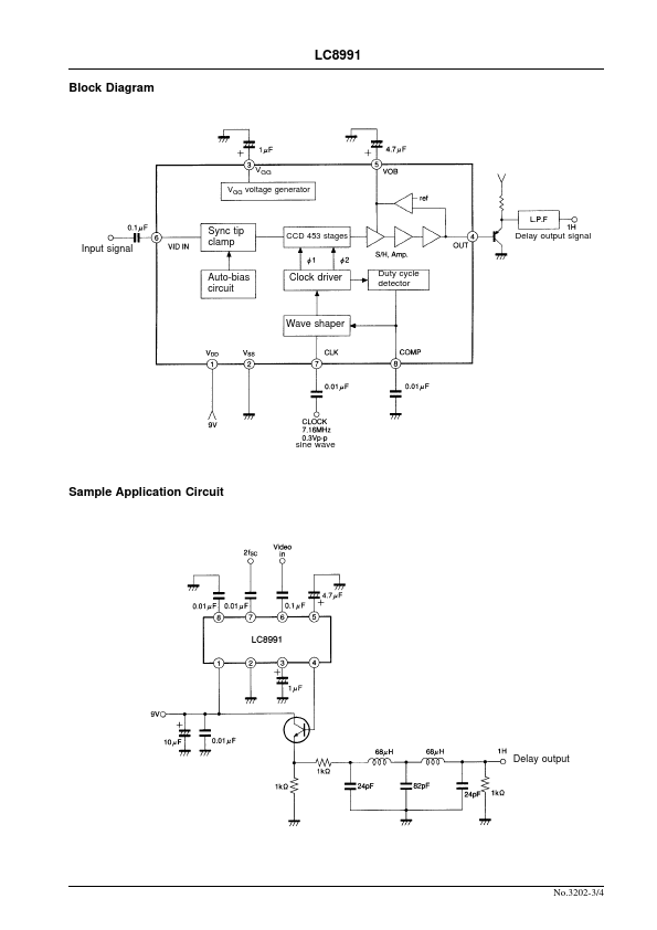
Functions
. 453 stages CCD shift register . CCD drive circuit . Auto-bias circuit . Sync tip clamp circuit
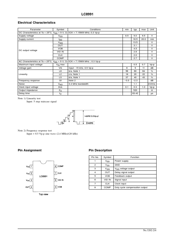
Specifications...