Datasheet4U Logo Datasheet4U.com

LC89962M - NTSC Format Delay Line

Datasheet Summary

Features

  • Requires only the input of a 3.58-MHz clock to produce a 1H delayed signal and the external low-pass filter.
  • Uses a 5-V single-voltage power supply.
  • Requires a minimal number of external components due to the peripheral components provided on chip.
  • Output signal has the same phase as the input signal.
  • Operation has a 4fsc clock synchronized with the input clock allows these products to be used as wide bandwidth delay lines.
  • A 4fsc clock.

📥 Download Datasheet

Datasheet preview – LC89962M

Datasheet Details

Part number LC89962M
Manufacturer Sanyo
File Size 98.34 KB
Description NTSC Format Delay Line
Datasheet download datasheet LC89962M Datasheet
Additional preview pages of the LC89962M datasheet.
Other Datasheets by Sanyo

Full PDF Text Transcription

Click to expand full text
Ordering number : EN*5420 CMOS LSI LC89962, LC89962M NTSC Format Delay Line Overview The LC89962 and LC89962M are delay line circuits that provide a delayed signal by a 1H period of NTSC format with an external low-pass filter. 
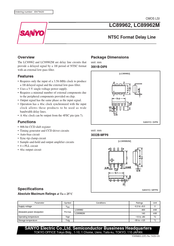
Package Dimensions unit: mm 3001B-DIP8 [LC89962] Features • Requires only the input of a 3.58-MHz clock to produce a 1H delayed signal and the external low-pass filter. • Uses a 5-V single-voltage power supply. • Requires a minimal number of external components due to the peripheral components provided on chip. • Output signal has the same phase as the input signal. • Operation has a 4fsc clock synchronized with the input clock allows these products to be used as wide bandwidth delay lines. • A 4fsc clock can be output from the 4FSC pin (pin 7).
Published: |