2N5619
Description
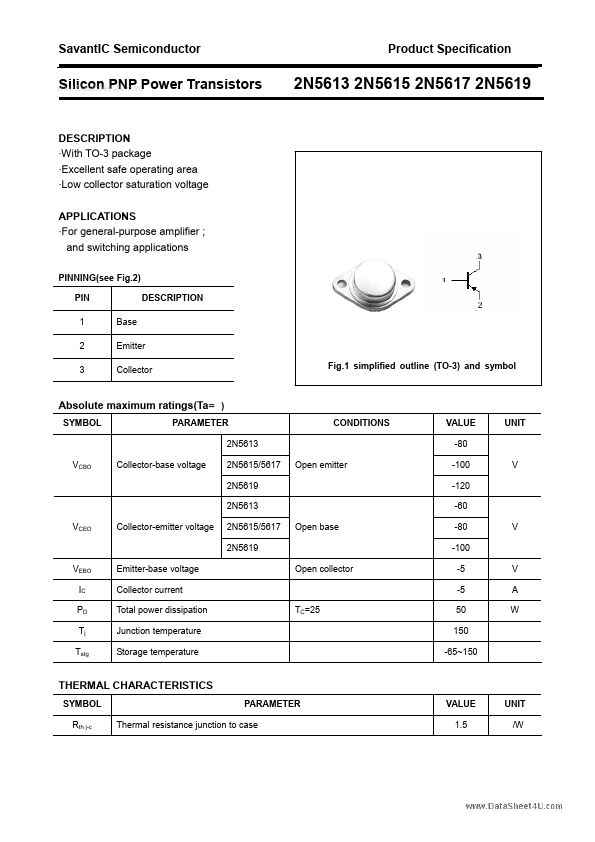
With TO-3 package - Excellent safe operating area - Low collector saturation voltage APPLICATIONS - For general-purpose amplifier ; and switching applications PINNING(see Fig.2) PIN 1 2 3 Base Emitter Collector Fig.1 simplified outline (TO-3) and symbol DESCRIPTION SYMBOL PARAMETER 2N5613 VCBO Collector-base voltage 2N5615/5617 2N5619 2N5613 VCEO Collector-emitter voltage 2N5615/5617 2N5619 VEBO IC PD Tj Tstg Emitter-base voltage Collector current Total power dissipation Junction temperature Storage temperature TC=25 Open collector Open base Open emitter CONDITIONS VALUE -80 -100 -120 -60 -80 -100 -5 -5 50 150 -65~150 V A W V V UNIT SYMBOL Rth j-c PARAMETER SavantIC Semiconductor.