2N5629
Description
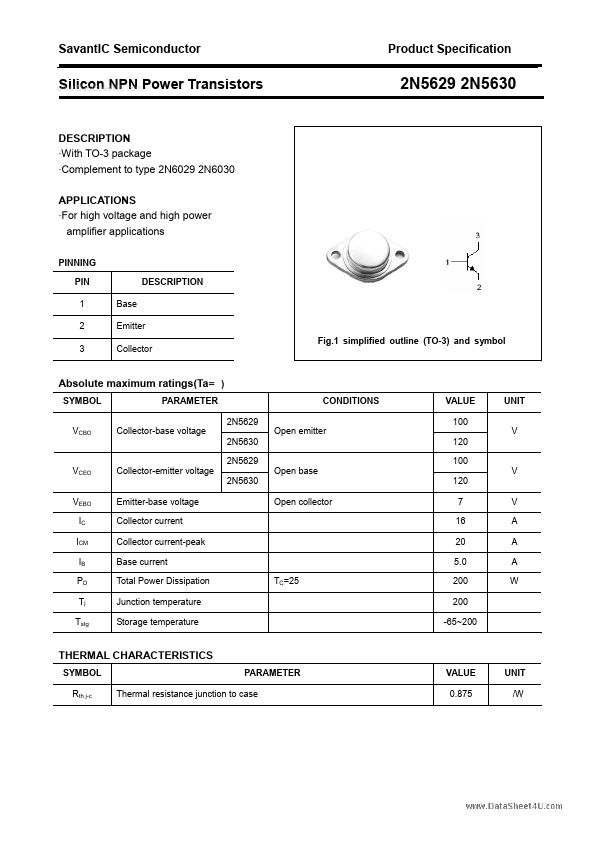
With TO-3 package - plement to type 2N6029 2N6030 APPLICATIONS - For high voltage and high power amplifier applications PINNING PIN 1 2 3 Base Emitter Collector Fig.1 simplified outline (TO-3) and symbol DESCRIPTION SYMBOL VCBO PARAMETER Collector-base voltage 2N5629 2N5630 Collector-emitter voltage Emitter-base voltage Collector current Collector current-peak Base current Total Power Dissipation Junction temperature Storage temperature TC=25 2N5629 2N5630 Open collector Open base CONDITIONS Open emitter VALUE 100 120 100 120 7 16 20 5.0 200 200 -65~200 V A A A W V UNIT V VCEO VEBO IC ICM IB PD Tj Tstg SYMBOL Rth j-c PARAMETER SavantIC Semiconductor.