Description
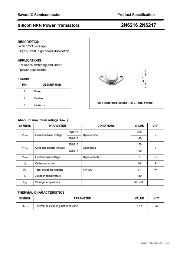
With TO-3 package - High current ,high power dissipation APPLICATIONS - For use in switching and linear power applications PINNING PIN 1 2 3 Base Emitter Collector Fig.1 simplified outline (TO-3) and symbol DESCRIPTION SYMBOL VCBO PARAMETER 2N6216 Collector-base voltage 2N6217 2N6216 VCEO VEBO IC PD Tj Tstg Collector-emitter voltage 2N6217 Emitter-base voltage Collector current Total power dissipation Junction temperature Storage temperature TC=100 Open collector Open base 140 7 10 71 150 -65~200 V A W Open emitter 180 150 V CONDITIONS VALUE 200 V UNIT SYMBOL Rth j-c PARAMETER SavantIC Semiconductor. Product Specification Silicon NPN Power Transistors CHARACTERISTICS Tj=25 unless otherwise specified PARAMETER 2N6216 IC=0.1A ;IB=0 2N6217 VCEsat-1 VCEsat-2 VBEsat Collector-emitter saturation voltage Collector-emitter saturation voltage Base-emitter saturation voltage 2N6216 ICEO Collector cut-off current 2N6217 ICBO IEBO hFE fT Collector cut-off current Emitter cut-off current DC current gain Transition frequency VCE=70V; IB=0 VCB=RatedVCBO; IE=0 VEB=7V; IC=0 IC=5A ; VCE=5V IC=1A ; VCE=10V IC=4A; IB=0.4A IC=6A; IB=0.75A IC=6A; IB=0.75A VCE=80V; IB=0 CONDITIONS 2N6216 2N6217 SYMBOL MIN 150 TYP.