2SC1610
DESCRIPTION
- With TO-3 package
- High current capability
- Fast switching speed APPLICATIONS
- For high speed power switching applications
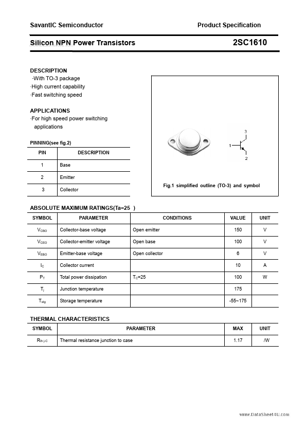
PINNING(see fig.2) PIN 1 2 3 Base Emitter Collector Fig.1 simplified outline (TO-3) and symbol DESCRIPTION
ABSOLUTE MAXIMUM RATINGS(Ta=25 )
SYMBOL VCBO VCEO VEBO IC PT Tj Tstg PARAMETER Collector-base voltage Collector-emitter voltage Emitter-base voltage Collector current Total power dissipation Junction temperature Storage temperature TC=25 Open emitter Open base Open collector CONDITIONS VALUE 150 100 6 10 100 175 -55~175 UNIT V V V A W
THERMAL CHARACTERISTICS
SYMBOL Rth j-C PARAMETER Thermal resistance junction to case MAX 1.17 UNIT /W
Savant IC Semiconductor
..
Product Specification
Silicon NPN Power Transistors
CHARACTERISTICS
Tj=25 unless otherwise specified PARAMETER Collector-emitter sustaining voltage Collector-base breakdown voltage Emitter-base breakdown voltage Collector-emitter saturation voltage Base-emitter saturation voltage...