2SC2809
DESCRIPTION
- With TO-3PN package
- High speed switching
- High breakdown voltage
- Wide area of safe operation APPLICATIONS
- For power amplifier applications PINNING
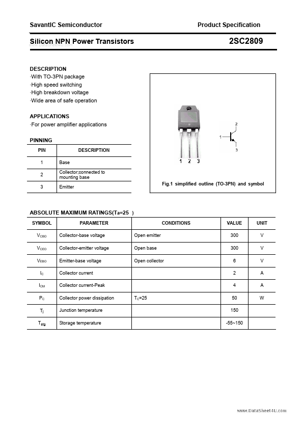
PIN 1 2 3 Base Collector;connected to mounting base Emitter Fig.1 simplified outline (TO-3PN) and symbol DESCRIPTION
ABSOLUTE MAXIMUM RATINGS(Ta=25 )
SYMBOL VCBO VCEO VEBO IC ICM PC Tj Tstg PARAMETER Collector-base voltage Collector-emitter voltage Emitter-base voltage Collector current Collector current-Peak Collector power dissipation Junction temperature Storage temperature TC=25 Open emitter Open base Open collector CONDITIONS VALUE 300 300 6 2 4 50 150 -55~150 UNIT V V V A A W
Savant IC Semiconductor
..
Product Specification
Silicon NPN Power Transistors
CHARACTERISTICS
Tj=25 unless otherwise specified PARAMETER Collector-emitter breakdown voltage Emitter-base breakdown voltage Collector-emitter saturation voltage Base-emitter saturation voltage Collector cut-off current Emitter cut-off current DC current gain...