A1105 Overview
Description
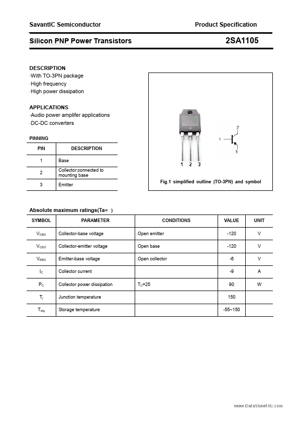
With TO-3PN package - High frequency - High power dissipation APPLICATIONS - Audio power amplifer applications - DC-DC converters PINNING PIN 1 2 3 Base Collector;connected to mounting base Emitter Fig.1 simplified outline (TO-3PN) and symbol DESCRIPTION SYMBOL VCBO VCEO VEBO IC PC Tj Tstg PARAMETER Collector-base voltage Collector-emitter voltage Emitter-base voltage Collector current Collector power dissipation Junction temperature Storage temperature TC=25 CONDITIONS Open emitter Open base Open collector VALUE -120 -120 -6 -9 90 150 -55~150 UNIT V V V A W SavantIC Semiconductor Product Specification Silicon PNP Power Transistors CHARACTERISTICS Tj=25 unless otherwise specified PARAMETER CONDITIONS MIN 2SA1105 SYMBOL TYP. MAX UNIT V(BR)CEO Collector-emitter breakdown voltage IC=-25mA ;IB=0 -120 V VCEsat Collector-emitter saturation voltage IC=-3A; IB=-0.3A -1.5 V VBEsat Base-emitter saturation voltage IC=-3A; IB=-0.3A -1.8 V ICBO Collector cut-off current VCB=-120V; IE=0 -100 µA IEBO Emitter cut-off current VEB=-6V; IC=0 -100 µA hFE DC current gain IC=-3A ; VCE=4V 50 180 fT Transition frequency IE=1A ; VCE=-12V 20 MHz 2 SavantIC Semiconductor Product Specification Silicon PNP Power Transistors PACKAGE OUTLINE 2SA1105 Fig.2 outline dimensions (unindicated tolerance:±0.1mm) 3.