A1250 Overview
Key Specifications
Mount Type: Panel
Height: 12.83 mm
Length: 26.19 mm
Max Operating Temp: 85 °C
Description
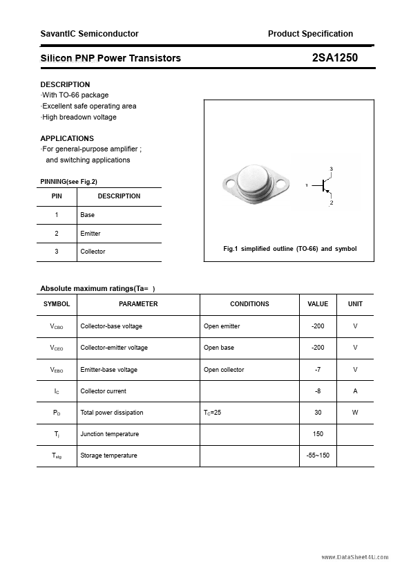
With TO-66 package - Excellent safe operating area - High breadown voltage APPLICATIONS - For general-purpose amplifier ; and switching applications PINNING(see Fig.2) PIN 1 2 3 Base Emitter Collector DESCRIPTION 2SA1250 Fig.1 simplified outline (TO-66) and symbol SYMBOL VCBO VCEO VEBO IC PD Tj Tstg PARAMETER Collector-base voltage Collector-emitter voltage Emitter-base voltage Collector current Total power dissipation Junction temperature Storage temperature TC=25 CONDITIONS Open emitter Open base Open collector VALUE -200 -200 -7 -8 30 150 -55~150 UNIT V V V A W Datasheet pdf - SavantIC Semiconductor Product Specification Silicon PNP Power Transistors CHARACTERISTICS Tj=25 unless otherwise specified PARAMETER CONDITIONS MIN 2SA1250 SYMBOL TYP. MAX UNIT V(BR)CEO V(BR)EBO VCEsat VBEsat ICBO IEBO hFE-1 hFE-2 Collector-emitter breakdown voltage IC=-10mA ;IB=0 IE=-1mA ;IC=0 IC=-5A; IB=-0.5A IC=-5A; IB=-0.5A VCB=200V; IE=0 VEB=-7V; IC=0 IC=-2A ; VCE=-1V IC=-5A ; VCE=-1V -200 V Emitter-base breakdown voltage -7 V Collector-emitter saturation voltage -1.5 V Base-emitter saturation voltage -2.0 V Collector cut-off current -10 µA Emitter cut-off current -10 µA DC current gain 40 200 DC current gain 20 2 Datasheet pdf - SavantIC Semiconductor Product Specification Silicon PNP Power Transistors PACKAGE OUTLINE 2SA1250 Fig.2 outline dimensions 3 Datasheet pdf.