B645
B645 is manufactured by SavantIC.
SavantIC Semiconductor wSwiwl.iDcatoaSnheePt4NU.cPomPower Transistors
DESCRIPTION
- With TO-3 package
- High power dissipation
APPLICATIONS
- For power switching and general purpose applications
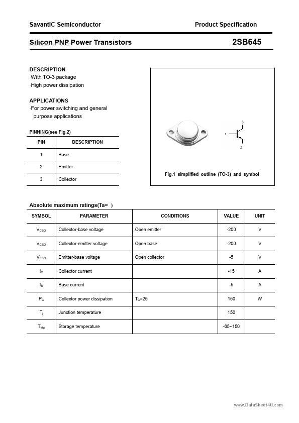
PINNING(see Fig.2) PIN DESCRIPTION 1 Base 2 Emitter 3 Collector
Product Specification
2SB645
Fig.1 simplified outline (TO-3) and...