BUV42 Overview
Key Specifications
Max Operating Temp: 200 °C
Description
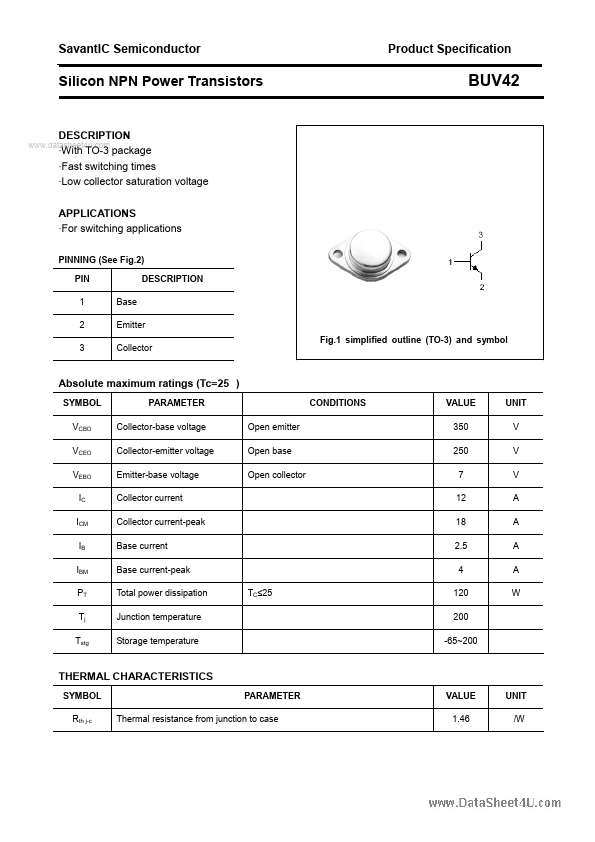
With TO-3 package - Fast switching times - Low collector saturation voltage APPLICATIONS - For switching applications PINNING (See Fig.2) PIN 1 2 3 Base Emitter Collector Fig.1 simplified outline (TO-3) and symbol DESCRIPTION SYMBOL VCBO VCEO VEBO IC ICM IB IBM PT Tj Tstg PARAMETER Collector-base voltage Collector-emitter voltage Emitter-base voltage Collector current Collector current-peak Base current Base current-peak Total power dissipation Junction temperature Storage temperature TC.25 Open emitter Open base Open collector CONDITIONS VALUE 350 250 7 12 18 2.5 4 120 200 -65~200 UNIT V V V A A A A W SYMBOL Rth j-c PARAMETER SavantIC Semiconductor Product Specification Silicon NPN Power Transistors CHARACTERISTICS Tj=25 unless otherwise specified PARAMETER CONDITIONS MIN TYP. BUV42 SYMBOL MAX UNIT VCEO(SUS) V(BR)EBO VCEsat-1 VCEsat-2 VCEsat-3 VBEsat-1 VBEsat-2 ICEV IEBO Collector-emitter sustaining voltage IC=0.2A ; L=25mH IE=50mA; IC=0 IC=2A; IB=0.13A Tj=100 IC=4A; IB=0.4A Tj=100 IC=6A; IB=0.75A Tj=100 IC=4A; IB=0.4A Tj=100 IC=6A; IB=0.75A Tj=100 VCE=VCEV; VBE=-1.5V TC=100 VEB=5V; IC=0 250 V Emitter-base breakdown voltage 7 0.8 0.9 0.9 1.2 1.2 1.5 1.3 V Collector-emitter saturation voltage V Collector-emitter saturation voltage V Collector-emitter saturation voltage V Base-emitter saturation voltage V Base-emitter saturation voltage 1.5 0.5 2.0 1 V Collector cut-off current mA Emitter cut-off current mA Switching times resistive load tr ts tf Rise time IC=6A ;IB1=0.75A RB2=3.3@; VCC=200V VBB=-5V; Tp=30µs 0.3 0.4 µs Storage time 1.0 1.6 µs Fall time 0.15 0.3 µs 2 SavantIC Semiconductor Product Specification Silicon NPN Power Transistors PACKAGE OUTLINE www.d.