C1942
C1942 is 2SC1942 manufactured by SavantIC.
Savant IC Semiconductor
Silicon NPN Power Transistors
..
DESCRIPTION
- With TO-3 package
- High breakdown voltage
- High speed switching
APPLICATIONS
- For TV horizontal output applications
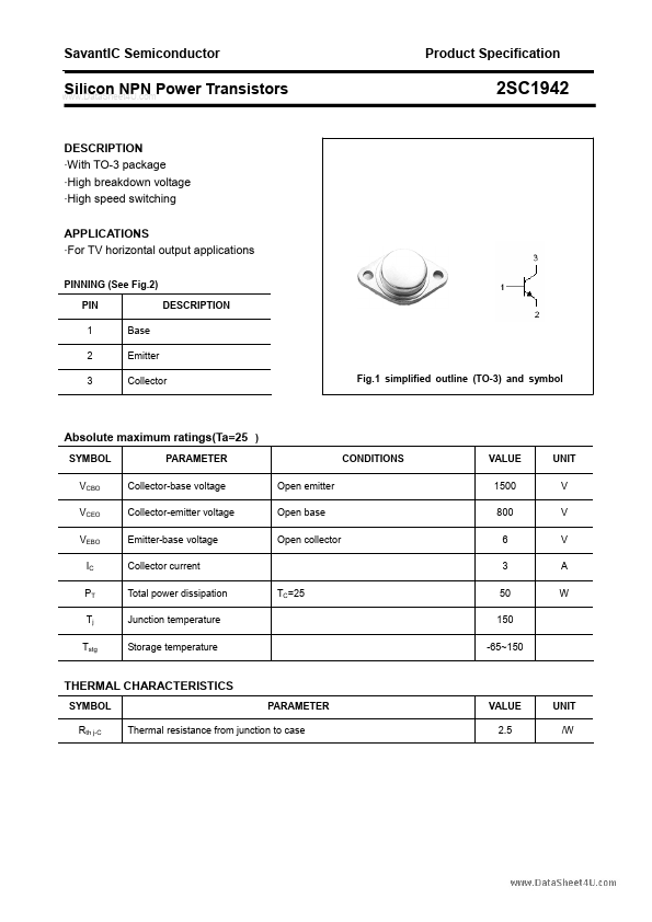
PINNING (See Fig.2) PIN DESCRIPTION 1 Base 2 Emitter 3 Collector
Product Specification
2SC1942
Fig.1 simplified outline (TO-3) and...